
A54SX08A-1TQ144
| Part Description |
SX-A Field Programmable Gate Array (FPGA) IC 113 144-LQFP |
|---|---|
| Quantity | 1,073 Available (as of June 15, 2026) |

| Product Category | Field Programmable Gate Array (FPGA) |
|---|---|
| Manufacturer | Microchip Technology |
| Manufacturing Status | Obsolete |
| Manufacturer Standard Lead Time | Contact Us |
| Datasheet |
Specifications & Environmental
| Device Package | 144-TQFP (20x20) | Grade | Commercial | Operating Temperature | 0°C – 70°C | ||
|---|---|---|---|---|---|---|---|
| Package / Case | 144-LQFP | Number of I/O | 113 | Voltage | 2.25 V - 5.25 V | ||
| Mounting Method | Surface Mount | RoHS Compliance | RoHS non-compliant | REACH Compliance | REACH Unaffected | ||
| Moisture Sensitivity Level | 3 (168 Hours) | Number of LABs/CLBs | 768 | Number of Logic Elements/Cells | 768 | ||
| Number of Gates | 12000 | ECCN | 3A991D | HTS Code | 8542.39.0001 | ||
| Qualification | N/A |
Overview of A54SX08A-1TQ144 – SX-A Field Programmable Gate Array (FPGA) IC 113 144-LQFP
The A54SX08A-1TQ144 is a commercial-grade SX-A family FPGA from Microchip Technology, delivered in a 144-pin thin/LQFP package. It provides a nonvolatile, single-chip FPGA solution with 12,000 system gates and 768 logic elements suited for designs that require flexible I/O, configurable timing, and on-chip nonvolatile configuration.
Targeted at system designs requiring mixed-voltage I/O and PCI-capable interfaces, this device combines dedicated flip-flop resources, 113 user I/Os, and a wide supply range to support a variety of embedded applications within a 0 °C to 70 °C operating window.
Key Features
- Core Capacity 12,000 system gates and 768 logic elements (logic modules) for implementing mid-density logic and control functions.
- Flip-Flop Resources Up to 2,012 dedicated flip-flops available in the SX-A family architecture for register-heavy designs.
- I/O and Mixed-Voltage Support 113 user I/Os in the 144-pin package; configurable I/O support for 3.3 V / 5 V PCI, 5 V TTL, 3.3 V LVTTL and 2.5 V LVCMOS2 with 5 V input tolerance and 5 V drive strength options documented by the family.
- Performance Family-level performance indicators include up to 250 MHz system performance and up to 350 MHz internal performance as specified for the SX-A family.
- Nonvolatile Single-Chip Configuration Nonvolatile architecture removes the need for external configuration memory and supports Power-Up/Down friendly operation without supply sequencing.
- Supply and Operating Range Voltage supply range of 2.25 V to 5.25 V and commercial temperature grading of 0 °C to 70 °C.
- System and Testability Boundary-scan testing compliant with IEEE 1149.1 (JTAG) and family support for in-system diagnostics and verification with Silicon Explorer II.
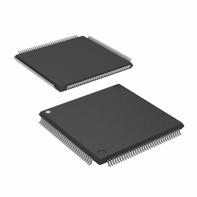
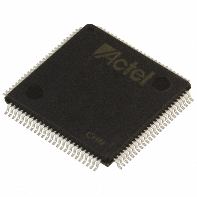
- Package and Mounting Surface-mount 144-pin package (144-LQFP / supplier device package 144-TQFP, 20×20 mm) for compact board layouts.
- Low-Level I/O Controls Configurable weak pull-up/pull-down at power-up and individual output slew rate control options are available at the family level.
- Security Actel Secure Programming Technology with FuseLock™ for design protection and prevention of reverse engineering (family feature).
- On-Chip Memory No embedded RAM bits (Total Ram Bits: 0) as specified for this device.
Typical Applications
- PCI Interface Logic Use where 66 MHz PCI compliance and configurable I/O voltage support are required to implement PCI endpoints or bridges.
- Mixed-Voltage System Glue Ideal for interfacing between 5 V and lower-voltage domains thanks to configurable I/O standards and 5 V input tolerance.
- Embedded Control and Timing Nonvolatile single-chip FPGA with deterministic, user-controllable timing and a significant flip-flop resource set for control, sequencing, and timing-critical logic.
Unique Advantages
- Nonvolatile, single-chip solution: Eliminates external configuration memory and simplifies power sequencing for more robust system startup.
- Flexible I/O voltage options: Built-in support for multiple I/O standards (3.3 V/5 V PCI, 5 V TTL, 3.3 V LVTTL, 2.5 V LVCMOS2) and 5 V input tolerance enable broad board-level interfacing without additional level shifters.
- Configurable timing and deterministic behavior: Family-level deterministic, user-controllable timing gives designers tighter control over timing closure and system behavior.
- Design protection features: FuseLock™ secure programming technology provides a hardware-level option to prevent reverse engineering of the programmed design.
- Compact package with ample I/O: 144-pin LQFP/TQFP packaging delivers 113 user I/Os for mid-density designs in space-constrained applications.
- Test and debug support: Boundary-scan (IEEE 1149.1) and in-system diagnostics with Silicon Explorer II help streamline bring-up and manufacturing test.
Why Choose A54SX08A-1TQ144?
The A54SX08A-1TQ144 offers a balanced combination of mid-range logic capacity, extensive configurable I/O, and nonvolatile single-chip configuration in a commercial-grade package. Its 12,000 system gates, 768 logic elements, 113 I/Os, and family-level performance characteristics make it well suited for embedded control, mixed-voltage interfacing, and PCI-capable system logic where reliable startup and in-field security are important.
Engineers and procurement teams looking for a compact FPGA solution with deterministic timing control, testability via JTAG, and vendor-backed secure programming capabilities will find this device appropriate for a wide range of commercial electronic designs operating across a 2.25 V to 5.25 V supply range and 0 °C to 70 °C environment.
Request a quote or contact sales to discuss availability, pricing, and how the A54SX08A-1TQ144 can be integrated into your next design.


Date Founded: 1989
Headquarters: Chandler, Arizona, USA
Employees: 22,000+
Revenue: $8.349 Billion
Certifications and Memberships: ISO9001:2015, IATF16949:2016, AS 9100D


