
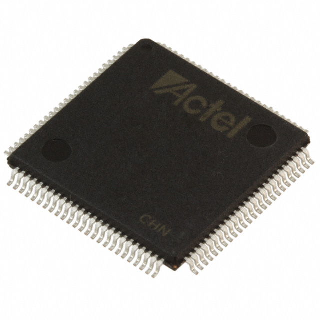
A54SX08A-2TQG100
| Part Description |
SX-A Field Programmable Gate Array (FPGA) IC 81 100-LQFP |
|---|---|
| Quantity | 381 Available (as of June 18, 2026) |

| Product Category | Field Programmable Gate Array (FPGA) |
|---|---|
| Manufacturer | Microchip Technology |
| Manufacturing Status | Active |
| Manufacturer Standard Lead Time | 12 Weeks |
| Datasheet |
Specifications & Environmental
| Device Package | 100-TQFP (14x14) | Grade | Commercial | Operating Temperature | 0°C – 70°C | ||
|---|---|---|---|---|---|---|---|
| Package / Case | 100-LQFP | Number of I/O | 81 | Voltage | 2.25 V - 5.25 V | ||
| Mounting Method | Surface Mount | RoHS Compliance | ROHS3 Compliant | REACH Compliance | REACH Unaffected | ||
| Moisture Sensitivity Level | 3 (168 Hours) | Number of LABs/CLBs | 768 | Number of Logic Elements/Cells | 768 | ||
| Number of Gates | 12000 | ECCN | 3A991D | HTS Code | 8542.39.0001 | ||
| Qualification | N/A |
Overview of A54SX08A-2TQG100 – SX-A FPGA, 81 I/O, 100-LQFP
The A54SX08A-2TQG100 is a nonvolatile SX-A family field programmable gate array from Microchip Technology. It provides 12,000 system gates implemented as approximately 768 logic elements with up to 81 user-programmable I/O pins in a 100-pin thin quad flat pack (100-LQFP) surface-mount package.
Designed for commercial-temperature embedded designs, this device targets applications that require configurable I/O, deterministic timing, and single-chip nonvolatile FPGA functionality with flexible mixed-voltage I/O support and on-chip security options.
Key Features
- Core Capacity — 12,000 system gates implemented as approximately 768 logic elements and up to the device maximum of dedicated flip-flops as reported in the SX-A family tables.
- Performance — SX-A family performance characteristics listed in the product datasheet include up to 250 MHz system performance and up to 350 MHz internal performance.
- User I/O — 81 user-programmable I/O pins (package-dependent routing) with configurable I/O support for multiple signaling standards and mixed-voltage operation.
- Configurable I/O Voltage — Supports mixed-voltage operation including 2.5 V, 3.3 V, and 5 V operation and configurable I/O options listed for PCI, TTL, LVTTL and LVCMOS2 signaling in the SX-A family documentation.
- Supply and Power — Wide supply input range from 2.25 V to 5.25 V and power-up/down friendly behavior noted for the SX-A family (no special sequencing required for supply voltages).
- Nonvolatile Single-Chip Solution — On-chip, nonvolatile configuration memory as part of the SX-A family architecture (single-chip configuration).
- System and Design Features — Hot-swap compliant I/Os, 66 MHz PCI compliance noted for the family, deterministic user-controllable timing, and boundary-scan (JTAG) testing capability.
- Security and Diagnostics — Family-level secure programming technology with FuseLock™ and in-system diagnostic and verification capability with Silicon Explorer II (as documented for SX-A devices).
- Package & Mounting — 100-pin thin quad flat pack (100-LQFP / supplier package 100-TQFP 14×14); surface mount.
- Commercial Temperature Grade — Operating temperature range 0 °C to 70 °C; RoHS compliant.
Typical Applications
- Embedded control logic — Implement custom glue logic, state machines, and control functions using the device’s 12,000 system gates and 768 logic elements.
- Interface bridging and I/O expansion — Use the 81 configurable I/Os and mixed-voltage support to interface between different logic levels and peripheral buses.
- PCI and peripheral interfacing — SX-A family PCI compliance and configurable I/O make the device suitable for designs that incorporate 66 MHz PCI signaling and related peripheral logic.
- In-system verification and secure configurations — Leverage the family’s in-system diagnostic features and FuseLock programming to protect and validate designs in the field.
Unique Advantages
- Nonvolatile single-chip FPGA: Eliminates the need for external configuration memory, simplifying board design and power sequencing.
- Flexible mixed-voltage I/O: Supports 2.5 V, 3.3 V and 5 V operation with configurable I/O standards to ease integration with varied legacy and modern interfaces.
- Deterministic timing control: Family-level features provide user-controllable, deterministic timing useful for time-critical logic and interface implementations.
- On-chip security and diagnostics: Secure programming (FuseLock™) and Silicon Explorer II diagnostics help protect IP and verify operation during development and deployment.
- Compact surface-mount packaging: 100-pin TQFP/LQFP package provides a balance of I/O count and PCB footprint for space-constrained commercial designs.
- RoHS compliant: Conforms to RoHS requirements for environmental compliance in commercial products.
Why Choose A54SX08A-2TQG100?
The A54SX08A-2TQG100 positions itself as a practical, commercial-grade FPGA option within the SX-A family for designers who need a nonvolatile, single-chip programmable solution with up to 81 configurable I/Os and roughly 768 logic elements (12,000 system gates). Its mixed-voltage I/O capability, deterministic timing features, and built-in security and diagnostic options make it well-suited for embedded control, interface bridging, and PCI-related applications where a compact surface-mount FPGA is required.
For projects that require clear configuration control, on-board security, and the option to run mixed-voltage systems on a single device, this part offers an integrative platform aligned with the SX-A family specification set.
Request a quote or submit an inquiry to receive pricing, availability, and lead-time information for the A54SX08A-2TQG100.


Date Founded: 1989
Headquarters: Chandler, Arizona, USA
Employees: 22,000+
Revenue: $8.349 Billion
Certifications and Memberships: ISO9001:2015, IATF16949:2016, AS 9100D


