
A54SX08A-FTQ100
| Part Description |
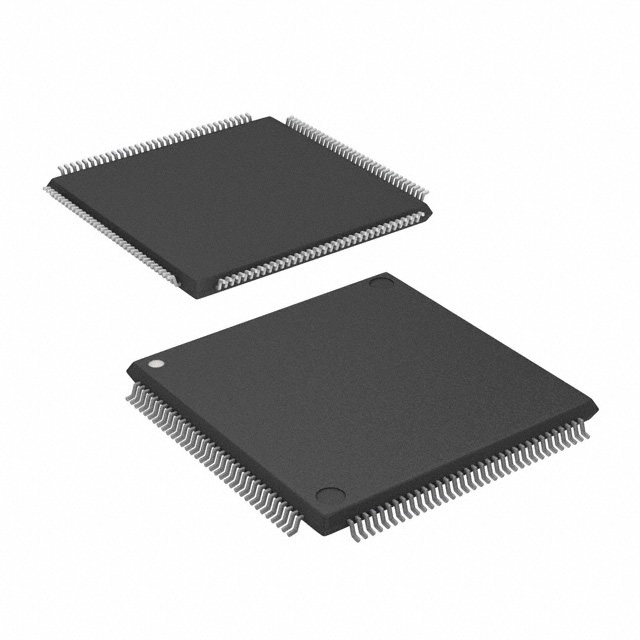
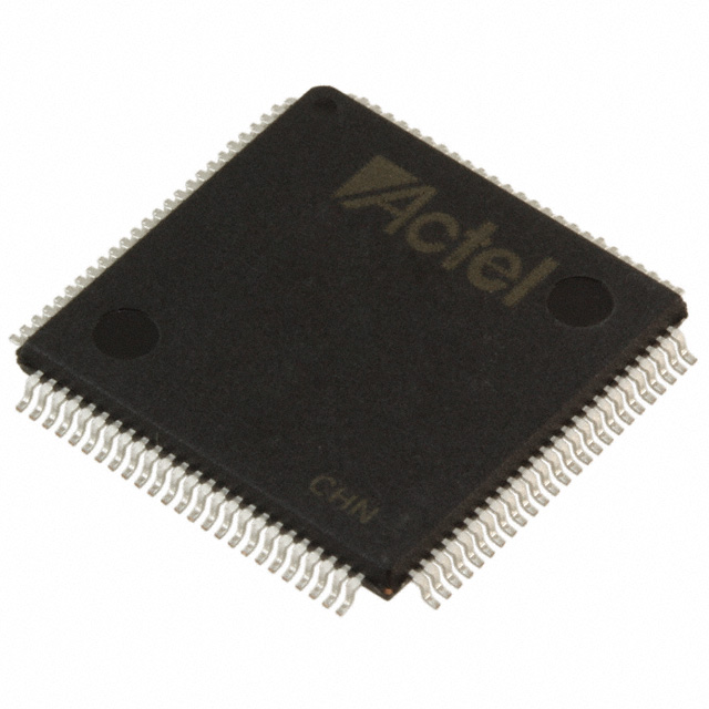
SX-A Field Programmable Gate Array (FPGA) IC 81 100-LQFP |
|---|---|
| Quantity | 386 Available (as of June 15, 2026) |

| Product Category | Field Programmable Gate Array (FPGA) |
|---|---|
| Manufacturer | Microchip Technology |
| Manufacturing Status | Obsolete |
| Manufacturer Standard Lead Time | Contact Us |
| Datasheet |
Specifications & Environmental
| Device Package | 100-TQFP (14x14) | Grade | Commercial | Operating Temperature | 0°C – 70°C | ||
|---|---|---|---|---|---|---|---|
| Package / Case | 100-LQFP | Number of I/O | 81 | Voltage | 2.25 V - 5.25 V | ||
| Mounting Method | Surface Mount | RoHS Compliance | RoHS non-compliant | REACH Compliance | REACH Unaffected | ||
| Moisture Sensitivity Level | 3 (168 Hours) | Number of LABs/CLBs | 768 | Number of Logic Elements/Cells | 768 | ||
| Number of Gates | 12000 | ECCN | 3A991D | HTS Code | 8542.39.0001 | ||
| Qualification | N/A |
Overview of A54SX08A-FTQ100 – SX-A Field Programmable Gate Array (FPGA) IC 81 100-LQFP
The A54SX08A-FTQ100 is a commercial-grade SX-A family FPGA from Microchip Technology provided in a 100-pin LQFP package (supplier device package: 100-TQFP, 14×14). It delivers mid-density programmable logic with 12,000 system gates and 768 logic elements for implementing control, glue logic and I/O-rich designs.
Built as a nonvolatile, single-chip FPGA solution, this device provides flexible mixed-voltage I/O, hot-swap compliant pins and deterministic timing capabilities for embedded systems, peripheral interfacing and system control applications that require a compact package and commercial temperature operation (0 °C to 70 °C).
Key Features
- Logic Capacity — 12,000 system gates and 768 logic elements, suitable for mid-density programmable logic implementations.
- I/O and Packaging — 81 user I/O pins in the 100-pin LQFP/TQFP package (14×14); configurable I/O supports multiple voltage standards and flexible drive options.
- Voltage and Temperature — Supply voltage range from 2.25 V to 5.25 V and commercial operating temperature range of 0 °C to 70 °C.
- Performance — Family-level performance indicators: up to 250 MHz system performance and 350 MHz internal performance.
- Nonvolatile Single-Chip Solution — On-chip nonvolatile configuration for single-chip deployments without external configuration memory.
- I/O Robustness — Hot-swap compliant I/Os, 5 V input tolerance and configurable weak pull-up/pull-down on power-up for safe interfacing and system-level robustness.
- System and Test Features — Boundary-scan testing in compliance with IEEE 1149.1 (JTAG) and support for deterministic, user-controllable timing.
- Security — Secure programming technology (FuseLock™) to prevent reverse engineering and protect design IP.
- Memory — Total on-chip RAM bits: 0 (no embedded RAM on this device).
- Standards — Family-level support for 66 MHz PCI signaling and mixed-voltage operation (2.5 V, 3.3 V and 5 V).
- Compliance — RoHS compliant.
Typical Applications
- Embedded Control — Implement control-state machines and peripheral interfaces where 768 logic elements and up to 81 I/Os provide the required integration in a compact package.
- Interface Bridging — Use the device’s mixed-voltage I/O, 5 V tolerance and flexible drive strength to bridge legacy 5 V peripherals with modern 3.3 V logic domains.
- Peripheral Glue Logic — Replace discrete logic with programmable logic to consolidate glue logic, enable in-field updates and reduce BOM in compact designs.
- Prototyping and Small-Scale Production — Suitable for prototyping and commercial-volume products that require a nonvolatile FPGA in a 100-pin LQFP/TQFP footprint.
Unique Advantages
- Compact, Deployable Package: 100-pin LQFP/TQFP footprint delivers mid-density logic and 81 I/Os in a small form factor for space-constrained boards.
- Nonvolatile, Single-Chip Implementation: Eliminates the need for external configuration memory, simplifying board design and improving system reliability.
- Flexible Voltage Support: Wide supply range (2.25 V to 5.25 V) and configurable I/O standards support mixed-voltage systems and ease integration with diverse peripherals.
- Robust I/O Behavior: Hot-swap compliance, 5 V input tolerance and configurable weak pull resistors at power-up reduce system-level sequencing constraints and simplify hot-plug scenarios.
- Security and Testability: FuseLock™ secure programming and IEEE 1149.1 boundary-scan support help protect IP and enable standard test flows.
- Predictable Performance: Family-level deterministic timing and high internal/system frequency capability support designs that require predictable, controllable timing margins.
Why Choose A54SX08A-FTQ100?
The A54SX08A-FTQ100 positions itself as a practical, nonvolatile FPGA option for commercial-temperature embedded designs that require mid-level logic capacity, flexible I/O and compact packaging. Its mix of hot-swap I/O features, wide supply voltage range and secure programming make it well suited to system control, interface bridging and glue logic consolidation in space-optimized boards.
For teams seeking a single-chip programmable solution with clear, verifiable specs—12,000 system gates, 768 logic elements, 81 I/Os, RoHS compliance and a 100-pin LQFP/TQFP footprint—this device provides a reliable platform with deterministic timing and standard test and security features to support product development and deployment.
Request a quote or submit an inquiry for pricing and availability to begin integrating the A54SX08A-FTQ100 into your next design.


Date Founded: 1989
Headquarters: Chandler, Arizona, USA
Employees: 22,000+
Revenue: $8.349 Billion
Certifications and Memberships: ISO9001:2015, IATF16949:2016, AS 9100D


