
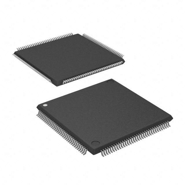
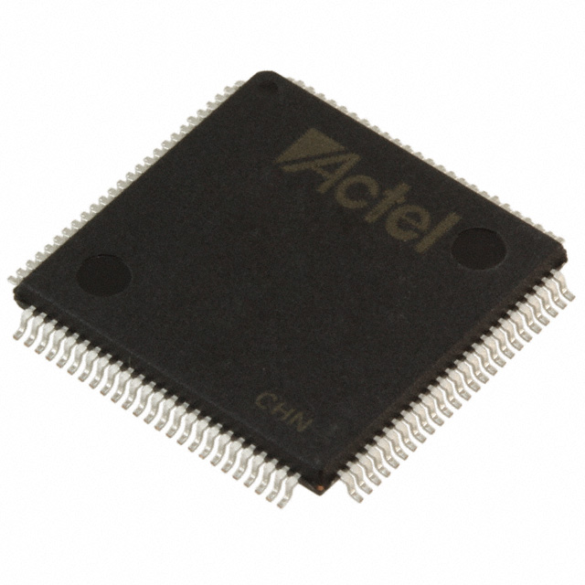
A54SX08A-TQ100
| Part Description |
SX-A Field Programmable Gate Array (FPGA) IC 81 100-LQFP |
|---|---|
| Quantity | 1,837 Available (as of June 15, 2026) |

| Product Category | Field Programmable Gate Array (FPGA) |
|---|---|
| Manufacturer | Microchip Technology |
| Manufacturing Status | Obsolete |
| Manufacturer Standard Lead Time | Contact Us |
| Datasheet |
Specifications & Environmental
| Device Package | 100-TQFP (14x14) | Grade | Commercial | Operating Temperature | 0°C – 70°C | ||
|---|---|---|---|---|---|---|---|
| Package / Case | 100-LQFP | Number of I/O | 81 | Voltage | 2.25 V - 5.25 V | ||
| Mounting Method | Surface Mount | RoHS Compliance | RoHS non-compliant | REACH Compliance | REACH Unaffected | ||
| Moisture Sensitivity Level | 3 (168 Hours) | Number of LABs/CLBs | 768 | Number of Logic Elements/Cells | 768 | ||
| Number of Gates | 12000 | ECCN | 3A991D | HTS Code | 8542.39.0001 | ||
| Qualification | N/A |
Overview of A54SX08A-TQ100 – SX-A Field Programmable Gate Array (FPGA) IC 81 100-LQFP
The A54SX08A-TQ100 is a commercial-grade FPGA from Microchip Technology's SX-A family. It provides a nonvolatile, single-chip programmable fabric with 12,000 system gates and approximately 768 logic elements for implementing custom digital functions.
Designed for mixed-voltage embedded designs, the device offers 81 user I/Os and flexible I/O configuration combined with a wide supply range, making it suitable for compact consumer and embedded-control applications that require in-field programmability and secure configuration.
Key Features
- Logic Capacity — 12,000 system gates and 768 logic elements provide the core resources to implement combinational and sequential logic for a variety of mid-range designs.
- User I/O — 81 user-programmable I/Os available in the 100-pin package allow interfacing to sensors, peripherals, and external buses.
- Nonvolatile Single-Chip Architecture — Built-in nonvolatile configuration removes the need for an external configuration memory, simplifying board-level design.
- Performance — Family-level performance characteristics include up to 250 MHz system performance and up to 350 MHz internal performance for timing-critical paths.
- Flexible I/O and Mixed-Voltage Support — Configurable I/O support and mixed-voltage operation (2.25 V to 5.25 V supply range) with 5 V input tolerance enable direct interfacing with common logic families and PCI signals.
- Package — 100-pin thin quad flat pack (TQFP) / 100-LQFP form factor (14 × 14 mm) for straightforward surface-mount assembly and compact PCB integration.
- Power and Reliability — Power-up/down friendly I/Os with configurable weak pull-up/pull-down options and individual output slew-rate control for signal integrity management.
- Security and Test — Family features include Secure Programming Technology (FuseLock™) to protect bitstreams and IEEE 1149.1 JTAG boundary-scan support for board-level testing and diagnostics.
- Environmental Compliance — RoHS-compliant device suitable for commercial product builds.
- Operating Range — Commercial temperature grade with an operating temperature range of 0 °C to 70 °C.
Typical Applications
- Embedded Control — Implements custom control logic, sequencing, and peripheral interfacing in compact embedded systems where nonvolatile configuration is preferred.
- Consumer Electronics — Provides programmable glue logic, protocol adaptation, and interface bridging in consumer devices with mixed-voltage I/O requirements.
- Prototyping and Development — Useful for hardware validation and firmware development where in-system programmability and diagnostic visibility are needed.
- PCI-Compatible Interfaces — Supports designs requiring 66 MHz PCI-compliant signaling and related interface logic through configurable I/O options.
Unique Advantages
- Nonvolatile, single-chip solution: Eliminates external configuration memory and simplifies BOM and board routing.
- Mixed-voltage flexibility: Wide supply range (2.25 V to 5.25 V) and configurable I/O allow direct interfacing to multiple logic families without extra level shifting.
- Compact package with ample I/O: 100-pin TQFP/LQFP balances small footprint with 81 user I/Os for dense, space-constrained designs.
- Built-in security and testability: FuseLock programming protection and IEEE 1149.1 boundary-scan support enhance IP protection and manufacturing test coverage.
- Deterministic timing and performance: Family-level timing and internal performance characteristics enable predictable timing closure for critical paths.
- RoHS-compliant commercial device: Meets common environmental requirements for consumer and commercial products.
Why Choose A54SX08A-TQ100?
The A54SX08A-TQ100 targets designers who need a compact, nonvolatile FPGA with moderate logic capacity and flexible I/O in a commercial-temperature device. Its combination of 12,000 system gates, approximately 768 logic elements, and 81 user I/Os in a 100-pin TQFP/LQFP package makes it a practical choice for mixed-voltage embedded designs, consumer products, and development platforms.
With built-in security features, JTAG test support, and configurable I/O behavior, the device helps reduce BOM complexity while providing the programmability and diagnostic visibility required for robust product development and deployment.
Request a quote or submit an inquiry to purchase the A54SX08A-TQ100 and learn about availability and lead times for your design needs.


Date Founded: 1989
Headquarters: Chandler, Arizona, USA
Employees: 22,000+
Revenue: $8.349 Billion
Certifications and Memberships: ISO9001:2015, IATF16949:2016, AS 9100D


