
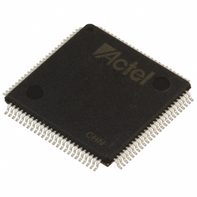
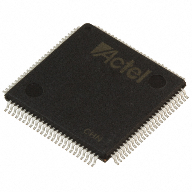
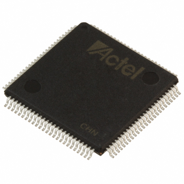
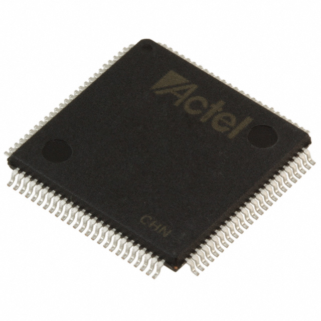
A54SX08A-TQ100A
| Part Description |
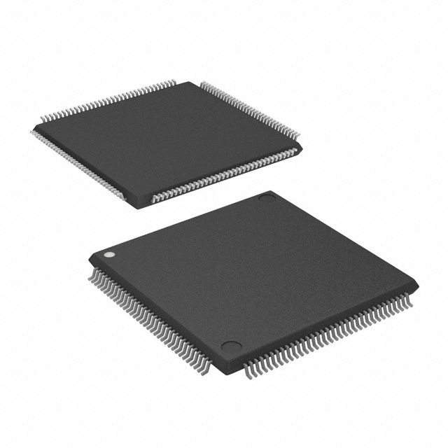
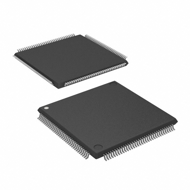
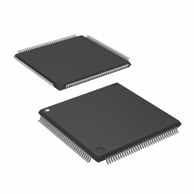
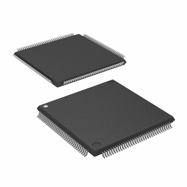
SX-A Field Programmable Gate Array (FPGA) IC 81 100-LQFP |
|---|---|
| Quantity | 1,424 Available (as of October 7, 2026) |
| Product Category | Field Programmable Gate Array (FPGA) |
|---|---|
| Manufacturer | Microchip Technology |
| Manufacturing Status | Obsolete |
| Manufacturer Standard Lead Time | Contact Us |
| Datasheet |
Specifications & Environmental
| Device Package | 100-TQFP (14x14) | Grade | Automotive | Operating Temperature | -40°C – 125°C | ||
|---|---|---|---|---|---|---|---|
| Package / Case | 100-LQFP | Number of I/O | 81 | Voltage | 2.25 V - 5.25 V | ||
| Mounting Method | Surface Mount | RoHS Compliance | RoHS non-compliant | REACH Compliance | REACH Unaffected | ||
| Moisture Sensitivity Level | 3 (168 Hours) | Number of LABs/CLBs | 768 | Number of Logic Elements/Cells | 768 | ||
| Number of Gates | 12000 | ECCN | 3A991D | HTS Code | 8542.39.0001 | ||
| Qualification | AEC-Q100 |
Overview of A54SX08A-TQ100A – SX-A Field Programmable Gate Array (FPGA) IC 81 100-LQFP
The A54SX08A-TQ100A is a nonvolatile SX-A family FPGA offered in a 100-pin LQFP package, designed for automotive-grade embedded systems. It combines a compact logic resource set with configurable I/O and a wide supply voltage range to address control, interfacing and secure configuration requirements in harsh environments.
Built to AEC‑Q100 qualification and RoHS compliance, this single-chip FPGA provides deterministic timing, configurable I/O standards and a surface-mount 100‑pin package for streamlined board-level integration.
Key Features
- Logic Capacity — 768 logic elements delivering approximately 12,000 system gates to implement control, glue-logic and custom digital functions.
- I/O Count & Configurability — 81 user I/Os with configurable I/O support; datasheet family features include compatibility with 3.3V PCI, 3.3V LVTTL and 2.5V LVCMOS2 signaling and hot-swap compliant I/Os.
- Nonvolatile Single-Chip Architecture — Nonvolatile configuration removes the need for external configuration memory and supports a single-chip solution for system designs.
- Voltage & Power — Wide supply voltage range from 2.25 V to 5.25 V and power-up/power-down friendly operation with no sequencing required for supply voltages.
- Performance & Timing — Family-spec performance characteristics include 250 MHz internal performance and deterministic, user-controllable timing for reliable timing closure.
- Security & Test — Family-level features include secure programming technology (FuseLock™) to protect intellectual property and IEEE 1149.1 (JTAG) boundary-scan support for production test.
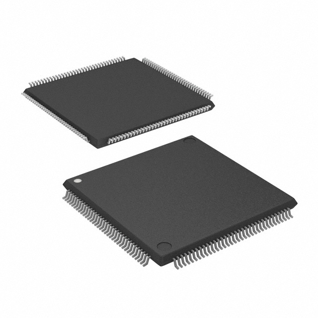
- Package & Mounting — 100‑pin LQFP package (supplier device package: 100‑TQFP, 14×14) in a surface-mount form factor for compact PCB designs.
- Automotive Qualification & Temperature Range — Automotive grade with AEC‑Q100 qualification and an operating temperature range of −40 °C to 125 °C.
- Regulatory Compliance — RoHS compliant.
Typical Applications
- Automotive control modules — Implement custom digital control and interfacing logic in AEC‑Q100 qualified designs requiring deterministic timing and nonvolatile configuration.
- Sensor interfacing — Aggregate and condition sensor signals using configurable I/O and dedicated logic resources in harsh temperature environments.
- Secure configuration and IP protection — Use nonvolatile configuration and FuseLock™ secure programming to protect design IP in production systems.
Unique Advantages
- Automotive-grade reliability: AEC‑Q100 qualification and a −40 °C to 125 °C operating range support deployment in temperature‑challenging automotive environments.
- Nonvolatile, single-chip solution: Eliminates the need for external configuration memory, simplifying BOM and system boot behavior.
- Flexible I/O and wide supply range: 81 configurable I/Os and a 2.25 V–5.25 V supply window enable easy interfacing with diverse system voltage domains.
- Deterministic timing and testability: User-controllable timing and JTAG boundary-scan support improve predictability in safety-critical designs and ease production test.
- Compact, surface-mount package: 100‑pin LQFP (100‑TQFP 14×14) provides a balance of I/O and small PCB footprint for space-constrained applications.
Why Choose A54SX08A-TQ100A?
The A54SX08A-TQ100A positions itself as a compact, automotive‑grade FPGA option that balances usable logic capacity with configurable I/O and robust qualification. Its nonvolatile, single-chip architecture and secure programming features make it suitable for embedded automotive designs that require stable configuration behavior and IP protection.
This device is well suited for designers seeking an AEC‑Q100 qualified FPGA with deterministic timing, a wide supply range and a small form-factor package to streamline system integration while meeting automotive environmental requirements.
Request a quote or submit a parts inquiry to evaluate the A54SX08A-TQ100A for your next design.





















Date Founded: 1989
Headquarters: Chandler, Arizona, USA
Employees: 22,000+
Revenue: $8.349 Billion
Certifications and Memberships: ISO9001:2015, IATF16949:2016, AS 9100D




