
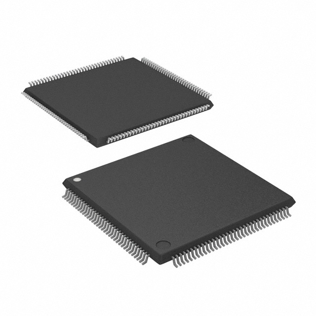
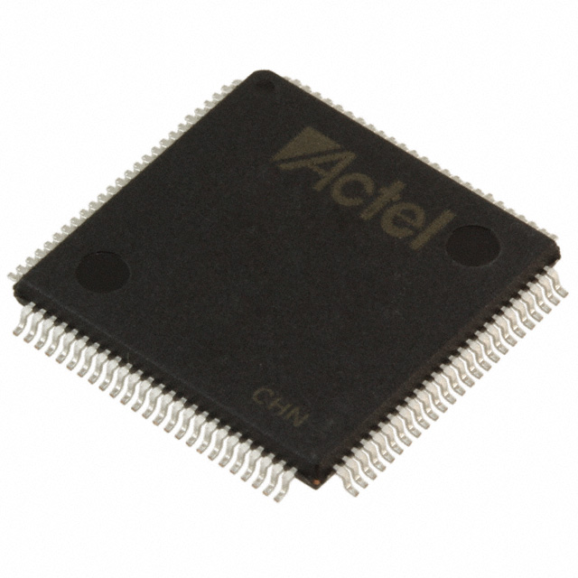
A54SX08A-TQ100I
| Part Description |
SX-A Field Programmable Gate Array (FPGA) IC 81 100-LQFP |
|---|---|
| Quantity | 1,148 Available (as of June 14, 2026) |

| Product Category | Field Programmable Gate Array (FPGA) |
|---|---|
| Manufacturer | Microchip Technology |
| Manufacturing Status | Obsolete |
| Manufacturer Standard Lead Time | Contact Us |
| Datasheet |
Specifications & Environmental
| Device Package | 100-TQFP (14x14) | Grade | Industrial | Operating Temperature | -40°C – 85°C | ||
|---|---|---|---|---|---|---|---|
| Package / Case | 100-LQFP | Number of I/O | 81 | Voltage | 2.25 V - 5.25 V | ||
| Mounting Method | Surface Mount | RoHS Compliance | RoHS non-compliant | REACH Compliance | REACH Unaffected | ||
| Moisture Sensitivity Level | 3 (168 Hours) | Number of LABs/CLBs | 768 | Number of Logic Elements/Cells | 768 | ||
| Number of Gates | 12000 | ECCN | 3A991D | HTS Code | 8542.39.0001 | ||
| Qualification | N/A |
Overview of A54SX08A-TQ100I – SX-A Field Programmable Gate Array (FPGA) IC 81 100-LQFP
The A54SX08A-TQ100I is an industrial-grade SX-A family FPGA from Microchip Technology provided in a 100-pin LQFP package. It delivers a nonvolatile, single-chip FPGA solution with 12,000 system gates and 768 logic elements for implementing glue logic, control functions and interface logic in industrial and embedded systems.
Built for mixed-voltage designs and PCI-capable systems, this device combines configurable I/O, deterministic timing features and in-system diagnostic support to simplify system integration and field verification.
Key Features
- Core Performance (SX-A family) Family-level performance includes up to 250 MHz system performance and up to 350 MHz internal performance, enabling responsive application-level logic and timing.
- Logic Resources 12,000 system gates and 768 logic elements provide capacity for mid-range logic implementations and control functions.
- I/O and Voltage Flexibility 81 user I/Os with configurable I/O support for 3.3 V / 5 V PCI, 5 V TTL, 3.3 V LVTTL and 2.5 V LVCMOS2; supports mixed-voltage operation with 5 V input tolerance and 5 V drive strength.
- No Embedded RAM Total on-chip RAM bits: 0 — useful to plan external memory if required by the design.
- Power and Hot-Swap Friendly 2.25 V to 5.25 V supply range and power-up/down friendly behavior (no supply sequencing required). I/Os are hot-swap compliant.
- Security and Testability Nonvolatile single-chip architecture with Actel Secure Programming Technology (FuseLock™) to protect intellectual property; boundary-scan testing supported (IEEE 1149.1 JTAG).
- Package and Temperature 100-pin LQFP package (supplier device package listed as 100-TQFP 14×14) and industrial temperature grade: -40 °C to +85 °C.
- In-System Diagnostics Family supports in-system diagnostic and verification capability (Silicon Explorer II) for field verification and debugging.
- Standards Support SX-A family devices support 66 MHz PCI compliance and deterministic, user-controllable timing for predictable system behavior.
- RoHS Compliant Device is RoHS compliant.
Typical Applications
- Industrial control and automation Use the A54SX08A-TQ100I for control logic, I/O interfacing and deterministic timing in industrial systems operating across -40 °C to +85 °C.
- PCI and legacy-system interfaces The device’s 66 MHz PCI compliance and configurable I/O levels make it well suited for PCI-compliant interface functions and legacy bus bridging.
- Embedded glue logic Implement board-level glue logic, protocol adaptation and peripheral control where a nonvolatile single-chip FPGA simplifies the bill of materials.
- Field-updatable systems In-system diagnostic and verification capabilities support field updates and hardware verification during maintenance operations.
Unique Advantages
- Nonvolatile single-chip design: Eliminates external configuration memory and simplifies system boot-up and supply sequencing.
- Mixed-voltage I/O flexibility: Configurable I/O standards and 5 V tolerance reduce level-shifting components and ease integration with diverse peripherals.
- Industrial temperature rating: Rated for -40 °C to +85 °C operation, supporting deployment in industrial environments.
- Security features: FuseLock™ programming technology for protection against reverse engineering and design theft.
- Testability and diagnostics: Boundary-scan (IEEE 1149.1) and in-system diagnostic support aid manufacturing test and field verification.
- Wide supply tolerance: Operation from 2.25 V to 5.25 V for flexible power-rail integration.
Why Choose A54SX08A-TQ100I?
The A54SX08A-TQ100I provides a focused mid-range FPGA option for embedded and industrial designs that need a nonvolatile, single-chip programmable device with flexible I/O and robust diagnostic features. Its combination of 12,000 system gates, 768 logic elements, PCI support and industrial temperature rating makes it a practical choice for board-level glue logic, interface bridging and field-updatable control applications.
Designed for engineers who require deterministic timing, configurable I/O levels and hardware protection features, this SX-A family device offers a balance of integration and system-level reliability while simplifying power sequencing and configuration management.
Request a quote or inquire about availability and lead times to discuss pricing and delivery for the A54SX08A-TQ100I.


Date Founded: 1989
Headquarters: Chandler, Arizona, USA
Employees: 22,000+
Revenue: $8.349 Billion
Certifications and Memberships: ISO9001:2015, IATF16949:2016, AS 9100D


