
A54SX16-TQG176I
| Part Description |
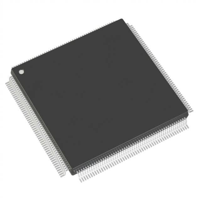
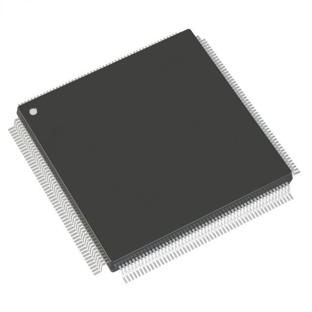
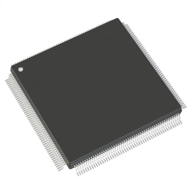
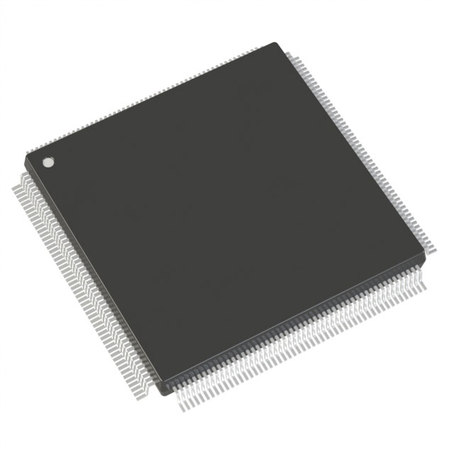
SX Field Programmable Gate Array (FPGA) IC 147 176-LQFP |
|---|---|
| Quantity | 1,208 Available (as of October 8, 2026) |

| Product Category | Field Programmable Gate Array (FPGA) |
|---|---|
| Manufacturer | Microchip Technology |
| Manufacturing Status | Active |
| Manufacturer Standard Lead Time | 12 Weeks |
| Datasheet |
Specifications & Environmental
| Device Package | 176-TQFP (24x24) | Grade | Industrial | Operating Temperature | -40°C – 85°C | ||
|---|---|---|---|---|---|---|---|
| Package / Case | 176-LQFP | Number of I/O | 147 | Voltage | 3 V - 5.5 V | ||
| Mounting Method | Surface Mount | RoHS Compliance | ROHS3 Compliant | REACH Compliance | REACH Unaffected | ||
| Moisture Sensitivity Level | 3 (168 Hours) | Number of LABs/CLBs | 1452 | Number of Logic Elements/Cells | 1452 | ||
| Number of Gates | 24000 | ECCN | 3A991D | HTS Code | 8542.39.0001 | ||
| Qualification | N/A |
Overview of A54SX16-TQG176I – SX FPGA, 24,000 System Gates, 1,452 Logic Elements
The A54SX16-TQG176I is a nonvolatile SX family Field Programmable Gate Array (FPGA) from Microchip Technology designed for industrial applications. It delivers a compact, single‑chip programmable logic solution ideal for control, interface and glue‑logic tasks that require deterministic timing and mixed‑voltage I/O support.
With 24,000 system gates and 1,452 logic elements, this device targets designs that need a mid‑density FPGA in a 176‑pin thin quad flat package, supported across a 3.0 V to 5.5 V supply range and an industrial temperature rating.
Key Features
- Core Performance — Family-level performance includes up to 250 MHz system performance and up to 350 MHz internal performance for timing‑sensitive logic implementations.
- Resources — 24,000 system gates and 1,452 logic elements with 147 user I/Os; device reports 0 bits of on‑chip RAM.
- Configurable I/O & Mixed-Voltage Operation — Supports configurable I/O standards including 3.3 V/5 V PCI, 5 V TTL, 3.3 V LVTTL and 2.5 V LVCMOS2; devices support 2.5 V, 3.3 V and 5 V mixed‑voltage operation with 5 V input tolerance and 5 V drive strength.
- Power and Reliability — Hot‑swap compliant I/Os and power‑up/power‑down friendly operation (no sequencing required for supply voltages) simplify system power management.
- Security and Test — Actel Secure Programming Technology with FuseLock™ protects design IP; boundary‑scan testing compliant with IEEE 1149.1 (JTAG) facilitates board‑level test.
- Deterministic Timing & Diagnostics — Deterministic, user‑controllable timing and unique in‑system diagnostic/verification capability with Silicon Explorer II provide predictable, debug‑friendly behavior.
- Package & Temperature — Available in a 176‑pin LQFP/TQFP package (supplier package 176‑TQFP, 24 × 24 mm) with an industrial operating temperature range of –40 °C to 85 °C.
- Compliance — RoHS compliant.
Typical Applications
- Industrial Control — Implement motor control timing, I/O aggregation, and deterministic control logic within industrial automation equipment operating across standard industrial temperature ranges.
- Interface Bridging — Bridge between mixed‑voltage buses and legacy 3.3 V/5 V signal domains for protocol conversion and glue logic.
- Embedded Systems — Provide mid‑density programmable logic for system control, peripheral management, and custom logic functions where nonvolatile single‑chip configuration is required.
- Test & Measurement — Use in test fixtures and instrumentation that benefit from in‑system diagnostics and boundary‑scan testability for board‑level validation.
Unique Advantages
- Nonvolatile Single‑Chip Solution: Eliminates the need for external configuration memory and simplifies system boot behavior.
- Mixed‑Voltage Flexibility: Broad I/O standard support and 5 V tolerance allow easy integration with legacy and modern logic families, reducing interface translation hardware.
- Industrial Temperature Rating: Rated for –40 °C to 85 °C, suitable for a wide range of industrial environments.
- Security and Testability: FuseLock™ secure programming and IEEE 1149.1 boundary‑scan support streamline production test and protect intellectual property.
- Deterministic Timing & Diagnostics: User‑controllable timing plus in‑system diagnostic tools support predictable system behavior and faster debug cycles.
- Compact Packaging: 176‑pin TQFP/LQFP footprint provides a balance of I/O density and PCB area efficiency for mid‑range designs.
Why Choose A54SX16-TQG176I?
The A54SX16-TQG176I positions itself as a practical, mid‑density FPGA solution for industrial designs that require nonvolatile configuration, mixed‑voltage I/O support and deterministic timing. Its combination of 24,000 system gates, 1,452 logic elements and 147 user I/Os in a 176‑pin package makes it well suited to control, interface and embedded applications where reliability and in‑system diagnostics matter.
Backed by Microchip Technology’s SX family features—secure programming, boundary‑scan testability and hot‑swap capable I/Os—this device delivers a stable platform for scalable designs that benefit from reduced BOM complexity and robust deployment in industrial environments.
Request a quote or submit an inquiry to receive pricing and availability for the A54SX16-TQG176I for your next design.




















Date Founded: 1989
Headquarters: Chandler, Arizona, USA
Employees: 22,000+
Revenue: $8.349 Billion
Certifications and Memberships: ISO9001:2015, IATF16949:2016, AS 9100D




