
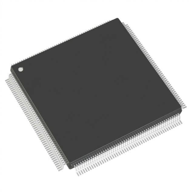
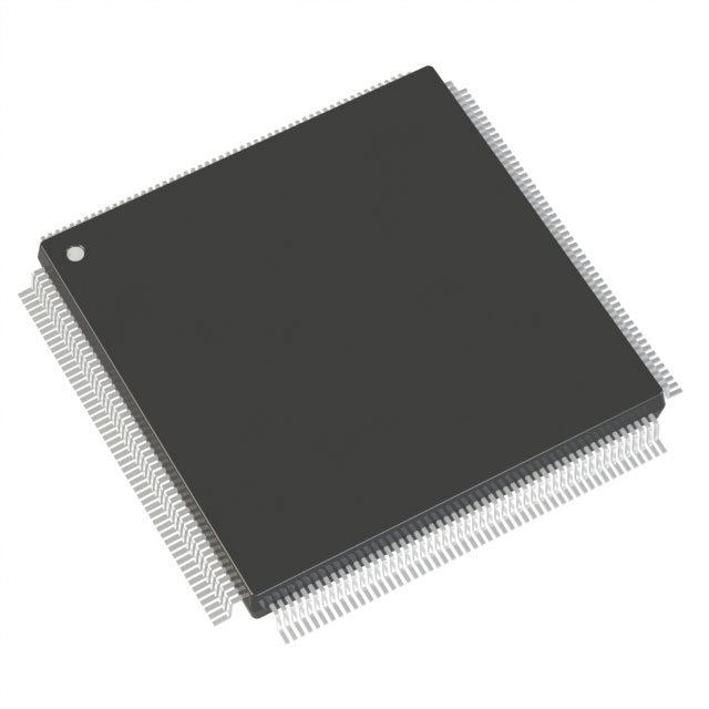
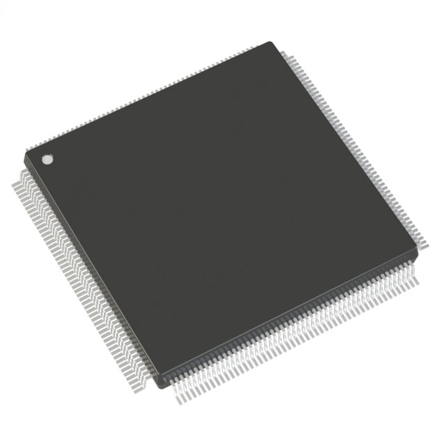
A54SX16-TQG176
| Part Description |
SX Field Programmable Gate Array (FPGA) IC 147 176-LQFP |
|---|---|
| Quantity | 1,609 Available (as of October 8, 2026) |

| Product Category | Field Programmable Gate Array (FPGA) |
|---|---|
| Manufacturer | Microchip Technology |
| Manufacturing Status | Active |
| Manufacturer Standard Lead Time | 12 Weeks |
| Datasheet |
Specifications & Environmental
| Device Package | 176-TQFP (24x24) | Grade | Commercial | Operating Temperature | 0°C – 70°C | ||
|---|---|---|---|---|---|---|---|
| Package / Case | 176-LQFP | Number of I/O | 147 | Voltage | 3 V - 5.25 V | ||
| Mounting Method | Surface Mount | RoHS Compliance | ROHS3 Compliant | REACH Compliance | REACH Unaffected | ||
| Moisture Sensitivity Level | 3 (168 Hours) | Number of LABs/CLBs | 1452 | Number of Logic Elements/Cells | 1452 | ||
| Number of Gates | 24000 | ECCN | 3A991D | HTS Code | 8542.39.0001 | ||
| Qualification | N/A |
Overview of A54SX16-TQG176 – SX Field Programmable Gate Array (FPGA) IC 147 176-LQFP
The A54SX16-TQG176 is a commercial-grade, nonvolatile SX-A family FPGA offered in a 176-pin thin QFP package. It provides a compact, surface-mount programmable logic solution with 24,000 system gates and 1,452 logic elements for embedded control, I/O aggregation, and custom glue-logic functions.
Designed for mixed-voltage systems, the device supports a wide supply range (3 V to 5.25 V), up to 147 user I/Os, and on-chip features that simplify board-level integration while preserving deterministic timing and in-system diagnostics.
Key Features
- Core Logic: 1,452 logic elements delivering approximately 24,000 system gates for implementing combinational and sequential logic in a compact FPGA.
- I/O Density and Flexibility: Up to 147 user I/Os with configurable I/O support for multiple voltage standards, enabling mixed-voltage interfacing on a single device.
- Voltage and Power: Operates from 3 V to 5.25 V and is power-up/power-down friendly with no supply sequencing required.
- Package and Mounting: 176-pin LQFP (thin QFP) surface-mount package (24 × 24 mm footprint) suitable for space-constrained board designs.
- Performance: Series-level performance characteristics include up to 250 MHz system performance and up to 350 MHz internal performance as documented for the SX-A family.
- Nonvolatile Single-Chip Solution: Built-in nonvolatile configuration memory removes external configuration dependencies and simplifies system boot behavior.
- System Reliability and Test: Hot-swap compliant I/Os, boundary-scan (IEEE 1149.1) support, and in-system diagnostic/verification capability referenced in the SX-A family documentation.
- Security: Series-level secure programming technology (FuseLock™) for protection against reverse engineering and unauthorized readout, as described in the family datasheet.
- Environmental Compliance: RoHS-compliant construction and commercial operating temperature range of 0 °C to 70 °C.
Typical Applications
- Embedded Control: Implement control logic, state machines, and custom peripherals where a compact, nonvolatile FPGA is required.
- Legacy and Bus Bridging: Support for PCI-related signaling and mixed-voltage I/O makes the device suitable for bridging legacy interfaces and peripheral buses.
- Communications and Networking Peripherals: Use as protocol glue, custom packet processing, or interface aggregation in communications equipment.
- Test and Measurement: On-chip deterministic timing and boundary-scan support facilitate development of instrumentation and bench-top test systems.
Unique Advantages
- Compact, High-Logic Density: 1,452 logic elements and 24,000 system gates in a 176-LQFP package reduce board area compared with multi-chip solutions.
- Mixed-Voltage I/O Support: Configurable I/Os and a wide supply range allow direct interfacing to 5 V and 3.3 V domains without extra level-shifting components.
- Nonvolatile Configuration: Single-chip nonvolatile architecture eliminates external configuration memory and simplifies system startup behavior.
- Design Security: Family-level secure programming (FuseLock™) provides protection against unauthorized design access and reverse engineering.
- Testability and Diagnostics: Boundary-scan (IEEE 1149.1) plus in-system diagnostic features help reduce bring-up time and ease board-level validation.
- Regulatory-Friendly: RoHS-compliant construction supports environmental directives for modern assemblies.
Why Choose A54SX16-TQG176?
The A54SX16-TQG176 combines a nonvolatile FPGA architecture with flexible mixed-voltage I/O and a compact 176-LQFP footprint to serve a wide range of commercial embedded applications. Its 1,452 logic elements and 24,000 system gates provide the capacity needed for glue logic, protocol handling, and peripheral consolidation while simplifying BOM and board complexity.
This device is well suited to designers seeking deterministic timing, in-system diagnostics, and secure programming features in a surface-mount package. With RoHS compliance and an established family feature set, the A54SX16-TQG176 offers a reliable, integrated building block for commercial electronics projects.
Request a quote or submit an inquiry to receive pricing and availability information for the A54SX16-TQG176.




















Date Founded: 1989
Headquarters: Chandler, Arizona, USA
Employees: 22,000+
Revenue: $8.349 Billion
Certifications and Memberships: ISO9001:2015, IATF16949:2016, AS 9100D




