
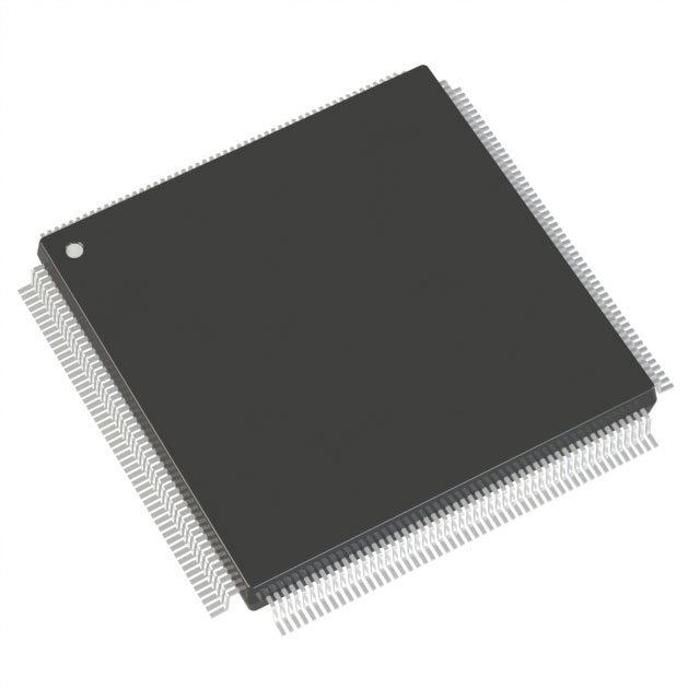
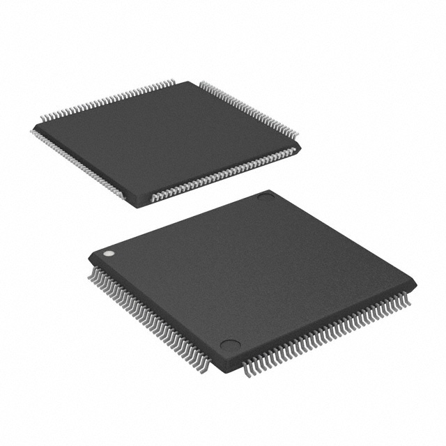
A54SX16-2TQG176
| Part Description |
SX Field Programmable Gate Array (FPGA) IC 147 176-LQFP |
|---|---|
| Quantity | 275 Available (as of June 14, 2026) |

| Product Category | Field Programmable Gate Array (FPGA) |
|---|---|
| Manufacturer | Microchip Technology |
| Manufacturing Status | Active |
| Manufacturer Standard Lead Time | 52 Weeks |
| Datasheet |
Specifications & Environmental
| Device Package | 176-TQFP (24x24) | Grade | Commercial | Operating Temperature | 0°C – 70°C | ||
|---|---|---|---|---|---|---|---|
| Package / Case | 176-LQFP | Number of I/O | 147 | Voltage | 3 V - 5.25 V | ||
| Mounting Method | Surface Mount | RoHS Compliance | ROHS3 Compliant | REACH Compliance | REACH Unaffected | ||
| Moisture Sensitivity Level | 3 (168 Hours) | Number of LABs/CLBs | 1452 | Number of Logic Elements/Cells | 1452 | ||
| Number of Gates | 24000 | ECCN | 3A991D | HTS Code | 8542.39.0001 | ||
| Qualification | N/A |
Overview of A54SX16-2TQG176 – SX Field Programmable Gate Array (FPGA) IC 147 176-LQFP
The A54SX16-2TQG176 is an SX-A family Field Programmable Gate Array (FPGA) from Microchip Technology, offered in a 176-pin LQFP/TQFP-style package. It delivers reconfigurable logic suitable for designs requiring a nonvolatile, single‑chip FPGA with mixed-voltage I/O capability and a compact surface‑mount footprint.
With approximately 24,000 system gates and 1,452 logic elements, this commercial‑grade device is targeted at embedded and interface applications that need flexible I/O, deterministic timing, and on‑chip flip‑flop resources in a 0 °C to 70 °C operating range.
Key Features
- Core Logic Approximately 24,000 system gates and 1,452 logic elements provide a mid-range logic capacity for combinational and sequential designs.
- User I/O Up to 147 user-programmable I/Os to support a variety of external signal interfaces in mixed-voltage systems.
- Voltage and Power Supports a supply range of 3 V to 5.25 V; datasheet references mixed-voltage operation including 2.5 V, 3.3 V, and 5 V signaling options and 5 V input tolerance.
- Nonvolatile Single‑Chip Architecture SX-A family architecture provides a nonvolatile, single‑chip FPGA implementation—no external configuration memory required.
- I/O Robustness and Control Hot-swap compliant I/Os, configurable weak pull-up/pull-down at power-up, and individual output slew rate control enable robust interfacing and signal integrity control.
- Package and Mounting Surface-mount 176-pin LQFP (supplier device package noted as 176-TQFP, 24×24) for compact board-level integration.
- Commercial Temperature Grade Rated for 0 °C to 70 °C operation for standard commercial applications.
- Compliance and Environmental RoHS compliant for environmentally conscious manufacturing and assembly.
- On‑chip Sequential Resources Dedicated flip‑flop resources and deterministic, user‑controllable timing enable predictable timing closure for synchronous designs.
- Test and Security Supports boundary-scan (JTAG) testing and secure programming technology for design protection and in-system diagnostics.
Typical Applications
- PCI and Bus Interface Logic Use where PCI‑compliant signaling and mid-range I/O counts are required to implement interface bridging, protocol glue logic, or peripheral controllers.
- Embedded Control Systems Suitable for embedded control tasks that need reconfigurable logic, deterministic timing, and a nonvolatile FPGA fabric without external configuration memory.
- Hot-Swap and Serviceable Systems Hot-swap compliant I/Os and configurable power-up behavior make this device appropriate for serviceable equipment and modular subsystems.
- Mixed‑Voltage Interfacing Ideal for designs that require interfacing between 5 V and 3.3 V domains with 5 V tolerant inputs and configurable I/O standards.
Unique Advantages
- Nonvolatile, single-chip solution: Eliminates the need for external configuration memory, reducing BOM count and board complexity.
- Flexible mixed-voltage I/O: Supports multiple I/O voltage levels and 5 V tolerance to simplify interfacing with legacy and modern peripherals.
- Compact surface-mount package: 176-pin LQFP/TQFP package provides a balance of pin density and board-level accessibility for mid-size designs.
- Deterministic timing and on-chip flip-flops: Provides predictable timing closure and sufficient sequential resources for synchronous designs.
- Design protection and test support: Secure programming technology and JTAG boundary-scan support help protect IP and facilitate in-system testing.
- RoHS compliant: Conforms to environmental requirements for modern manufacturing processes.
Why Choose A54SX16-2TQG176?
The A54SX16-2TQG176 delivers mid-range FPGA capacity—approximately 24,000 system gates and 1,452 logic elements—with up to 147 user I/Os in a compact 176-pin surface-mount package. Its nonvolatile SX-A family architecture, mixed-voltage I/O capability, and on-chip sequential resources make it well suited for embedded control, interface bridging, and systems that require reliable in-system configurability without external configuration memory.
Engineers designing commercial-temperature applications that need deterministic timing, robust I/O control, and reduced BOM complexity will find the A54SX16-2TQG176 a practical option. The device’s RoHS compliance and surface-mount package support modern manufacturing and assembly workflows.
Request a quote or submit an inquiry to purchase A54SX16-2TQG176 and get pricing and availability information.


Date Founded: 1989
Headquarters: Chandler, Arizona, USA
Employees: 22,000+
Revenue: $8.349 Billion
Certifications and Memberships: ISO9001:2015, IATF16949:2016, AS 9100D


