
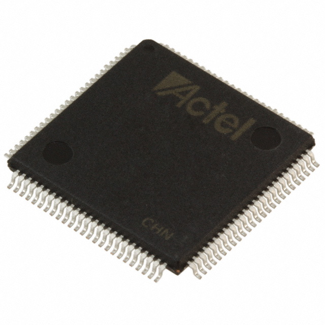
A54SX08A-TQG144I
| Part Description |
SX-A Field Programmable Gate Array (FPGA) IC 113 144-LQFP |
|---|---|
| Quantity | 334 Available (as of June 14, 2026) |

| Product Category | Field Programmable Gate Array (FPGA) |
|---|---|
| Manufacturer | Microchip Technology |
| Manufacturing Status | Active |
| Manufacturer Standard Lead Time | 12 Weeks |
| Datasheet |
Specifications & Environmental
| Device Package | 144-TQFP (20x20) | Grade | Industrial | Operating Temperature | -40°C – 85°C | ||
|---|---|---|---|---|---|---|---|
| Package / Case | 144-LQFP | Number of I/O | 113 | Voltage | 2.25 V - 5.25 V | ||
| Mounting Method | Surface Mount | RoHS Compliance | ROHS3 Compliant | REACH Compliance | REACH Unaffected | ||
| Moisture Sensitivity Level | 3 (168 Hours) | Number of LABs/CLBs | 768 | Number of Logic Elements/Cells | 768 | ||
| Number of Gates | 12000 | ECCN | 3A991D | HTS Code | 8542.39.0001 | ||
| Qualification | N/A |
Overview of A54SX08A-TQG144I – SX‑A FPGA, 12,000 System Gates, 113 I/O, Industrial Grade
The A54SX08A-TQG144I is a member of the SX‑A family of Field Programmable Gate Arrays from Microchip Technology. This nonvolatile, single‑chip FPGA delivers 12,000 system gates with 768 logic elements and 113 user I/O pins in a 144‑pin LQFP package.
Designed for industrial applications, the device supports a wide supply range (2.25 V to 5.25 V) and an operating temperature range of −40 °C to 85 °C. Family features include hot‑swap compliant I/Os, power‑up/power‑down friendly behavior, PCI compliance, boundary‑scan (JTAG) testing, and in‑system diagnostic capabilities.
Key Features
- Core & Capacity 12,000 system gates and 768 logic elements provide a compact programmable fabric for control, glue logic, and moderate‑complexity custom logic functions. The device does not include on‑chip RAM (Total RAM Bits: 0).
- Performance SX‑A family performance characteristics include documented system performance up to 250 MHz and internal performance up to 350 MHz as specified for the family.
- I/O and Mixed‑Voltage Support 113 user I/Os with configurable I/O support for 3.3 V / 5 V PCI, 5 V TTL, 3.3 V LVTTL and 2.5 V LVCMOS2. I/Os are hot‑swap compliant and provide 5 V input tolerance and 5 V drive strength where supported by the family.
- Power & Voltage Wide supply voltage range (2.25 V to 5.25 V) plus power‑up/power‑down friendliness—no sequencing required for supply voltages—simplifies power system design.
- Security & Test Family features include Actel Secure Programming Technology with FuseLock™ to deter reverse engineering and design theft, and boundary‑scan testing compliant with IEEE 1149.1 (JTAG).
- Diagnostics & Tools Unique in‑system diagnostic and verification capability with Silicon Explorer II (family feature) enables on‑board debug and verification.
- Package & Temperature 144‑pin LQFP package and industrial temperature grade (−40 °C to 85 °C) make the device suitable for industrial environments requiring robust thermal operation.
Typical Applications
- Industrial Control — Use the industrial temperature rating, wide supply range and 113 I/Os for sensor interfacing, actuator control and real‑time I/O aggregation in control systems.
- Embedded Systems — Nonvolatile single‑chip FPGA eliminates the need for external configuration memory and supports compact embedded designs that require retained configuration and field programmability.
- PCI and Legacy Bus Interfaces — The family’s 66 MHz PCI compliance and mixed‑voltage I/O support enable bridging and interface logic for PCI and 5 V legacy systems.
- Secure, Testable Designs — FuseLock programming and IEEE 1149.1 boundary‑scan support simplify manufacturing test and help protect intellectual property.
Unique Advantages
- Nonvolatile, single‑chip solution: Eliminates the need for external configuration memory and simplifies system boot and board-level BOM.
- Flexible mixed‑voltage I/O: Configurable I/O standards and 5 V tolerance allow direct interfacing to a broad range of legacy and modern logic levels.
- Industrial robustness: Wide supply voltage range and −40 °C to 85 °C operating range support deployment in industrial environments.
- Deterministic timing and full utilization: SX‑A family features include deterministic, user‑controllable timing and support for up to 100% resource utilization with pin locking.
- Built‑in security and testability: FuseLock programming and IEEE‑1149.1 boundary‑scan support help protect designs and streamline production testing.
- On‑board diagnostic capability: Silicon Explorer II in‑system diagnostics enable board‑level verification and debugging during development and in the field.
Why Choose A54SX08A-TQG144I?
The A54SX08A-TQG144I provides a compact, nonvolatile FPGA option for industrial and embedded designs that need reliable I/O, mixed‑voltage interfacing and on‑board configuration retention. With 12,000 system gates, 768 logic elements and 113 user I/Os in a 144‑pin LQFP package, the device balances capacity and footprint for control, interface and glue‑logic applications.
Its family‑level capabilities—hot‑swap I/Os, power‑up/power‑down friendly operation, JTAG boundary‑scan, secure programming and in‑system diagnostics—support robust board design, testability and IP protection while simplifying system integration.
Request a quote or contact sales to check pricing and availability for the A54SX08A-TQG144I and to discuss configuration, lead times and volume options.


Date Founded: 1989
Headquarters: Chandler, Arizona, USA
Employees: 22,000+
Revenue: $8.349 Billion
Certifications and Memberships: ISO9001:2015, IATF16949:2016, AS 9100D


