
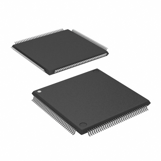
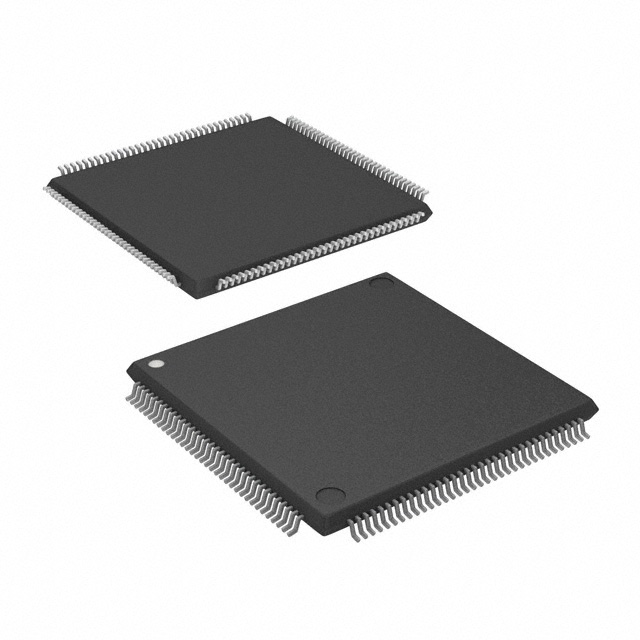
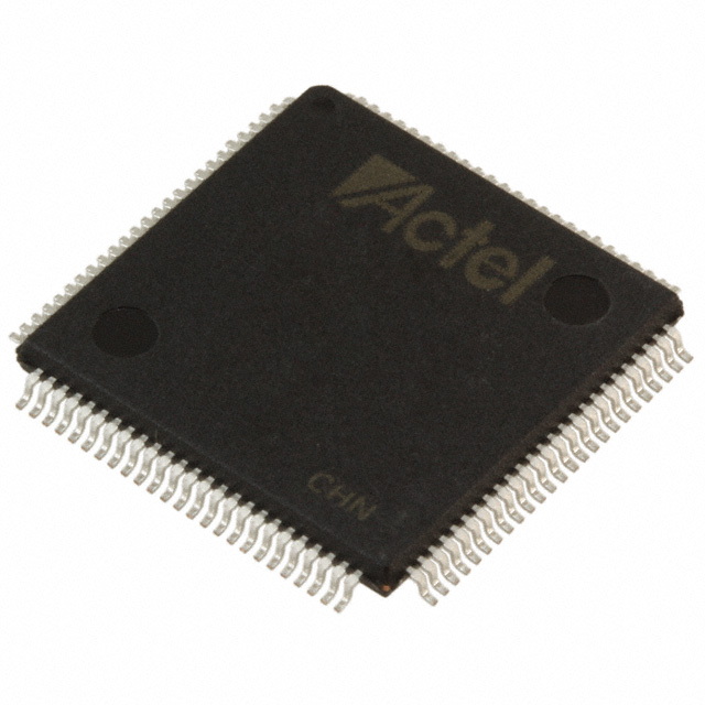
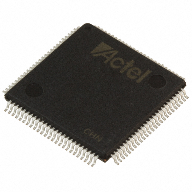
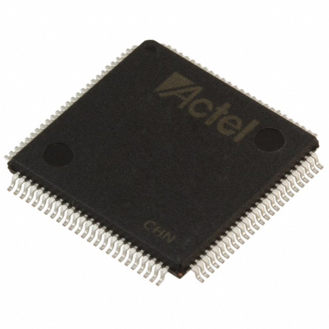
A54SX08A-TQG144A
| Part Description |
SX-A Field Programmable Gate Array (FPGA) IC 113 144-LQFP |
|---|---|
| Quantity | 640 Available (as of October 7, 2026) |
| Product Category | Field Programmable Gate Array (FPGA) |
|---|---|
| Manufacturer | Microchip Technology |
| Manufacturing Status | Active |
| Manufacturer Standard Lead Time | 12 Weeks |
| Datasheet |
Specifications & Environmental
| Device Package | 144-TQFP (20x20) | Grade | Automotive | Operating Temperature | -40°C – 125°C | ||
|---|---|---|---|---|---|---|---|
| Package / Case | 144-LQFP | Number of I/O | 113 | Voltage | 2.25 V - 5.25 V | ||
| Mounting Method | Surface Mount | RoHS Compliance | ROHS3 Compliant | REACH Compliance | REACH Unaffected | ||
| Moisture Sensitivity Level | 3 (168 Hours) | Number of LABs/CLBs | 768 | Number of Logic Elements/Cells | 768 | ||
| Number of Gates | 12000 | ECCN | 3A991D | HTS Code | 8542.39.0001 | ||
| Qualification | AEC-Q100 |
Overview of A54SX08A-TQG144A – SX-A Field Programmable Gate Array (FPGA) IC 113 144-LQFP
The A54SX08A-TQG144A is an automotive-grade SX-A family FPGA in a 144-pin LQFP package. It delivers a nonvolatile, single-chip programmable logic solution with approximately 12,000 system gates and 768 logic elements targeted at embedded and automotive applications.
Designed for robust operation, the device provides 113 user I/Os (TQFP 144-pin footprint), AEC-Q100 qualification, a wide supply range (2.25 V to 5.25 V) and an operating temperature range of −40 °C to 125 °C to meet demanding system requirements.
Key Features
- Core Capacity Approximately 12,000 system gates and 768 logic elements enable mid-range programmable logic implementations.
- Logic and Registers Dedicated flip-flops are available (device-specific values in the SX-A family datasheet) for deterministic sequential logic.
- I/O and Interface Support 113 user-programmable I/Os (144-pin TQFP footprint) with configurable support for 3.3 V PCI, 3.3 V LVTTL and 2.5 V LVCMOS2 signaling.
- Performance & Timing Up to 250 MHz internal performance and deterministic, user-controllable timing for predictable system behavior.
- Nonvolatile & System Integration Nonvolatile single-chip FPGA eliminates external configuration memory and provides a compact programmable solution.
- Power & Robustness Hot-swap compliant I/Os and power-up/power-down friendly operation (no sequencing required for supply voltages) simplify system power management.
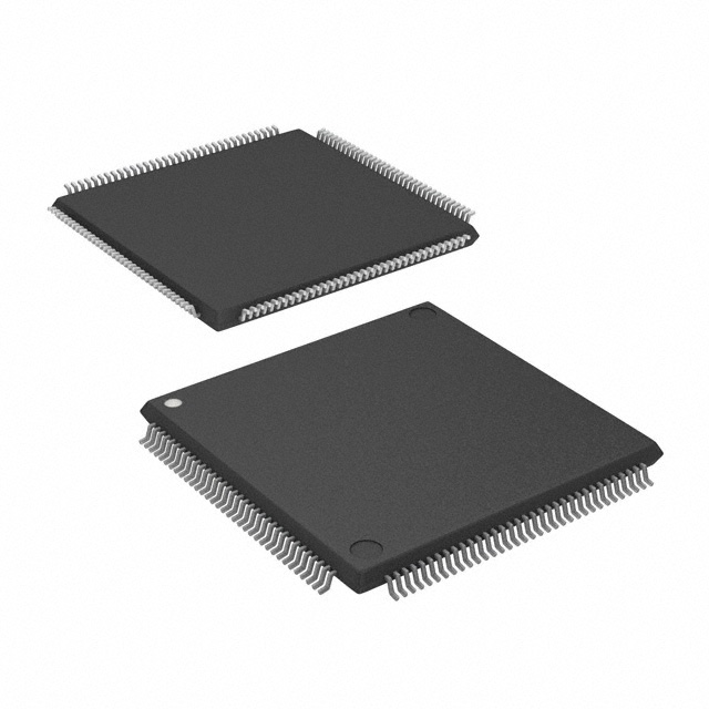
- Package & Environmental Surface-mount 144-LQFP package (supplier device package: 144-TQFP, 20×20) rated for −40 °C to 125 °C; RoHS compliant.
- Automotive Qualification AEC-Q100 qualification supports use in automotive-grade designs.
- Design Security & Test Series features include boundary-scan (IEEE 1149.1) and secure programming technology to protect designs and enable in-system diagnostics.
Typical Applications
- Automotive control systems AEC-Q100 qualification and wide operating temperature range make the device suitable for in-vehicle controllers and domain-specific logic.
- Sensor interfacing and signal conditioning Configurable I/O standards and a high I/O count support diverse sensor interfaces and custom front-end logic.
- PCI-based and legacy interface bridging 66 MHz PCI compliance and flexible I/O make the FPGA a fit for designs requiring PCI or LVTTL/LVCMOS2 interfacing.
- Embedded control and state machines Deterministic timing and dedicated flip-flops enable reliable implementation of control logic and finite-state machines.
Unique Advantages
- Automotive-ready qualification: AEC-Q100 qualification and −40 °C to 125 °C operating range support deployment in automotive environments.
- Nonvolatile single-chip solution: Eliminates the need for external configuration memory, simplifying board design and reducing component count.
- Flexible I/O standards: Configurable support for 3.3 V PCI, 3.3 V LVTTL and 2.5 V LVCMOS2 allows direct interfacing to a wide range of peripherals.
- Power-friendly behavior: Hot-swap compliant I/Os and no required supply sequencing ease system integration and power domain management.
- Predictable performance: Up to 250 MHz internal performance and user-controllable timing deliver predictable timing for critical logic.
Why Choose A54SX08A-TQG144A?
The A54SX08A-TQG144A positions itself as a compact, automotive-grade FPGA that combines nonvolatile single-chip programmability with mid-range logic capacity and flexible I/O. Its AEC-Q100 qualification, wide supply voltage range and extended temperature rating make it suitable for embedded systems where reliability and predictable timing are required.
This device is well suited to designers who need a programmable, in-system-configurable solution for automotive and embedded control applications, sensor interfaces, and PCI-compatible logic bridging—offering long-term robustness and a simplified BOM through integrated nonvolatile configuration.
Request a quote or submit an inquiry to our sales team to evaluate the A54SX08A-TQG144A for your next embedded or automotive design.





















Date Founded: 1989
Headquarters: Chandler, Arizona, USA
Employees: 22,000+
Revenue: $8.349 Billion
Certifications and Memberships: ISO9001:2015, IATF16949:2016, AS 9100D




