
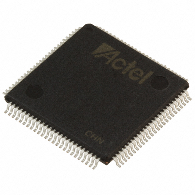
A54SX16-1TQG176
| Part Description |
SX Field Programmable Gate Array (FPGA) IC 147 176-LQFP |
|---|---|
| Quantity | 1,786 Available (as of June 18, 2026) |

| Product Category | Field Programmable Gate Array (FPGA) |
|---|---|
| Manufacturer | Microchip Technology |
| Manufacturing Status | Active |
| Manufacturer Standard Lead Time | 12 Weeks |
| Datasheet |
Specifications & Environmental
| Device Package | 176-TQFP (24x24) | Grade | Commercial | Operating Temperature | 0°C – 70°C | ||
|---|---|---|---|---|---|---|---|
| Package / Case | 176-LQFP | Number of I/O | 147 | Voltage | 3 V - 5.25 V | ||
| Mounting Method | Surface Mount | RoHS Compliance | ROHS3 Compliant | REACH Compliance | REACH Unaffected | ||
| Moisture Sensitivity Level | 3 (168 Hours) | Number of LABs/CLBs | 1452 | Number of Logic Elements/Cells | 1452 | ||
| Number of Gates | 24000 | ECCN | 3A991D | HTS Code | 8542.39.0001 | ||
| Qualification | N/A |
Overview of A54SX16-1TQG176 – SX Field Programmable Gate Array (147 I/O, 176-LQFP)
The A54SX16-1TQG176 is a commercial-grade SX family Field Programmable Gate Array (FPGA) supplied by Microchip Technology. It provides a nonvolatile, single-chip FPGA architecture with 24,000 system gates and approximately 1,452 logic elements, optimized for mixed-voltage I/O and in-system programmability.
With 147 user I/Os in a 176-pin surface-mount package and a wide supply range of 3 V to 5.25 V, this device targets designs that require flexible I/O interfacing, deterministic timing control, and embedded system integration at commercial temperatures (0 °C to 70 °C).
Key Features
- Core Capacity — Approximately 24,000 system gates and 1,452 logic elements provide a mid-range FPGA resource set for glue logic, control functions, and custom hardware implementation.
- Performance — SX family silicon delivers documented system and internal performance characteristics suitable for timing-sensitive designs, including high internal switching performance.
- I/O Flexibility — 147 user-programmable I/Os with configurable I/O support for multiple voltage domains and 5 V tolerant options as documented for the SX family.
- Mixed-Voltage Operation — Supports 2.5 V, 3.3 V, and 5 V mixed-voltage operation with 5 V input tolerance and drive capability as specified for the SX-A family.
- Nonvolatile Single-Chip Solution — On-chip nonvolatile configuration removes the need for external configuration memory, simplifying board-level design and system integration.
- Package & Mounting — Surface-mount 176-pin package (listed as 176-LQFP; supplier package noted as 176-TQFP, 24 × 24) for compact PCB layouts.
- Voltage & Temperature — Operates from 3 V to 5.25 V and rated for commercial temperature range of 0 °C to 70 °C.
- Design Security & Test — SX family includes features for boundary-scan (JTAG) and secure programming methods to protect designs and support production testability.
- RoHS Compliant — Device is listed as RoHS compliant for lead-free manufacturing environments.
Typical Applications
- Mixed-Voltage Interface Logic — Implement level translation, interface bridging, and custom I/O conditioning where 2.5 V, 3.3 V and 5 V domains must coexist.
- PCI and Legacy Bus Support — Suitable for control and glue logic in systems that require PCI-compatible I/O signaling and bus interfacing as described for the SX family.
- In-System Programmable Control — Use for in-circuit programmable state machines, peripheral control, and board-level system glue without external configuration ROM.
- Boundary-Scan and Production Test — Integrate into designs requiring IEEE 1149.1 (JTAG) boundary-scan for manufacturing test and debug.
Unique Advantages
- Nonvolatile single-chip architecture: Eliminates external configuration memory and simplifies board design and system boot-up.
- Flexible I/O with mixed-voltage support: Reduces the need for external level shifters by supporting multiple I/O voltage domains and 5 V tolerant inputs.
- Mid-range logic capacity: Approximately 1,452 logic elements and 24,000 system gates provide the right balance of integration for control, interface, and custom logic tasks.
- Compact surface-mount packaging: 176-pin LQFP/TQFP package options support high-density PCB layouts while providing up to 147 user I/Os.
- Design security and testability: Includes boundary-scan support and secure programming technology to protect intellectual property and aid production testing.
- RoHS compliant: Facilitates adoption in lead-free manufacturing environments.
Why Choose A54SX16-1TQG176?
The A54SX16-1TQG176 positions itself as a practical, commercial-grade FPGA solution for mid-complexity designs that need nonvolatile in-system programmability, flexible mixed-voltage I/O, and robust testability. Its combination of approximately 24,000 system gates, 1,452 logic elements, and 147 user I/Os in a 176-pin surface-mount package makes it well suited for interface logic, control functions, and embedded system glue where board-level simplification and configuration security matter.
For teams designing at commercial temperature ranges who require mixed-voltage operation (3 V–5.25 V) and RoHS compliance, this device offers a balance of integration, deterministic timing, and in-system programmability under a proven SX family feature set.
Request a quote or submit an inquiry to receive pricing and availability for the A54SX16-1TQG176.


Date Founded: 1989
Headquarters: Chandler, Arizona, USA
Employees: 22,000+
Revenue: $8.349 Billion
Certifications and Memberships: ISO9001:2015, IATF16949:2016, AS 9100D


