
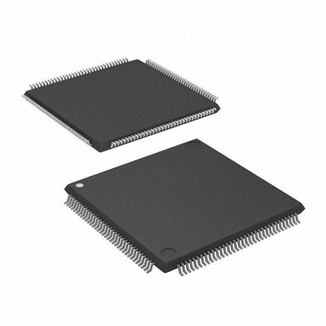
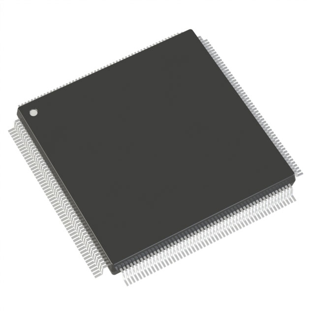
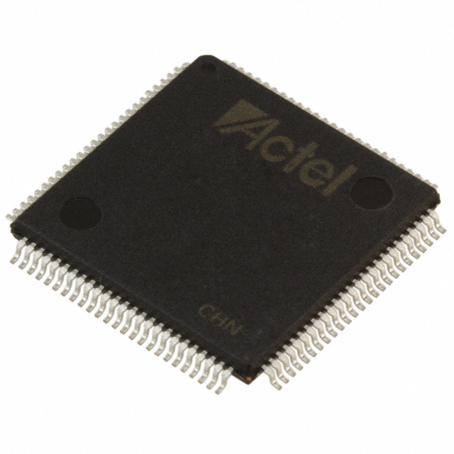
A54SX16A-PQ208
| Part Description |
SX-A Field Programmable Gate Array (FPGA) IC 175 208-BFQFP |
|---|---|
| Quantity | 1,742 Available (as of June 15, 2026) |

| Product Category | Field Programmable Gate Array (FPGA) |
|---|---|
| Manufacturer | Microchip Technology |
| Manufacturing Status | Obsolete |
| Manufacturer Standard Lead Time | Contact Us |
| Datasheet |
Specifications & Environmental
| Device Package | 208-PQFP (28x28) | Grade | Commercial | Operating Temperature | 0°C – 70°C | ||
|---|---|---|---|---|---|---|---|
| Package / Case | 208-BFQFP | Number of I/O | 175 | Voltage | 2.25 V - 5.25 V | ||
| Mounting Method | Surface Mount | RoHS Compliance | RoHS non-compliant | REACH Compliance | REACH Unaffected | ||
| Moisture Sensitivity Level | 3 (168 Hours) | Number of LABs/CLBs | 1452 | Number of Logic Elements/Cells | 1452 | ||
| Number of Gates | 24000 | ECCN | 3A991D | HTS Code | 8542.39.0001 | ||
| Qualification | N/A |
Overview of A54SX16A-PQ208 – SX-A Field Programmable Gate Array (FPGA) IC 175 208-BFQFP
The A54SX16A-PQ208 is a member of the SX-A family of nonvolatile, single-chip FPGAs. It provides 24,000 system gates, 1,452 logic elements and up to 175 user I/Os in a 208-pin quad-flat package for surface-mount board-level integration.
This device is designed for applications that require deterministic logic resources and flexible mixed-voltage I/O. Key electrical and environmental parameters include a voltage supply range of 2.25 V to 5.25 V and a commercial operating temperature range of 0 °C to 70 °C. The device is RoHS compliant.
Key Features
- Logic Capacity 24,000 system gates and 1,452 logic elements provide a defined resource set for mid-density digital designs.
- I/O and Interface Flexibility Up to 175 user I/Os with configurable support for mixed-voltage operation (2.5 V, 3.3 V, 5 V) and 5 V input tolerance and drive strength, simplifying interfacing with a range of peripheral devices and legacy buses.
- Nonvolatile, Single-Chip Configuration On-chip, nonvolatile configuration removes the need for external configuration memory and supports power-up/power-down friendly behavior without supply-sequencing requirements.
- Performance Characteristics SX-A family performance specifications include up to 250 MHz system performance and up to 350 MHz internal performance (family-level specification).
- Deterministic Timing & Debug Deterministic, user-controllable timing and in-system diagnostic/verification capability (Silicon Explorer II) help with predictable timing closure and field diagnostics (family-level features).
- Test and Security Boundary-scan testing compliant with IEEE 1149.1 (JTAG) and Actel Secure Programming Technology with FuseLock™ for protection against reverse engineering (family-level features).
- Package & Mounting 208-pin surface-mount quad-flat package (208-BFQFP / 208-PQFP, 28×28 mm footprint noted by supplier) for standard PCB assembly processes.
- Electrical & Environmental Voltage supply range: 2.25 V to 5.25 V. Operating temperature: 0 °C to 70 °C. RoHS compliant.
- Embedded Memory No on-chip RAM bits (Total RAM bits: 0), enabling designs that rely on logic and external memory resources.
Typical Applications
- Mixed-Voltage Interface Designs Use the device to bridge or interface between 5 V and 3.3 V logic domains where 5 V tolerance and mixed-voltage support are required.
- PCI and Bus-Based Subsystems Family-level PCI compliance and abundant I/Os make the device suitable for subsystem logic on boards implementing 66 MHz PCI-compatible interfaces.
- Embedded Control and Glue Logic Mid-density gate count and plentiful I/Os enable integration of control functions, protocol translation, and glue logic to reduce external components.
Unique Advantages
- Highly Integrated Logic Resources: 24,000 system gates and 1,452 logic elements consolidate mid-density logic into a single package, reducing PCB area and BOM complexity.
- Nonvolatile Configuration: Built-in, single-chip nonvolatile configuration removes the need for external configuration PROMs, simplifying system power-up behavior.
- Flexible Mixed-Voltage I/O: Configurable I/O and 5 V tolerance enable direct interfacing with a wide range of peripherals and legacy interfaces without level shifters.
- Design Visibility and Test: Boundary-scan (IEEE 1149.1) and in-system diagnostics (Silicon Explorer II capability at the family level) help streamline manufacturing test and field troubleshooting.
- Security Options: FuseLock secure programming technology (family feature) provides a hardware-based option to protect intellectual property.
- Commercial Temperature and RoHS Compliance: Commercial-grade operating range (0 °C to 70 °C) and RoHS compliance support standard electronics production and regulatory requirements.
Why Choose A54SX16A-PQ208?
The A54SX16A-PQ208 positions itself as a mid-density, nonvolatile FPGA option within the SX-A family, delivering a balanced combination of logic capacity, I/O density and mixed-voltage interfacing. Its single-chip nonvolatile configuration and family-level features for deterministic timing, JTAG boundary-scan and secure programming make it suitable for designs that need stable configuration behavior and I/O flexibility.
This device is a fit for engineers and procurement teams specifying commercial-temperature FPGA solutions for embedded control, bus-interface logic and mixed-voltage subsystems. Family-level tool and programming capabilities provide a clear upgrade path within the SX-A family for designs that may scale across different capacity points.
Request a quote or submit an inquiry today to get pricing and availability for the A54SX16A-PQ208 and to discuss quantity, lead time and integration considerations.


Date Founded: 1989
Headquarters: Chandler, Arizona, USA
Employees: 22,000+
Revenue: $8.349 Billion
Certifications and Memberships: ISO9001:2015, IATF16949:2016, AS 9100D


