
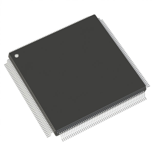
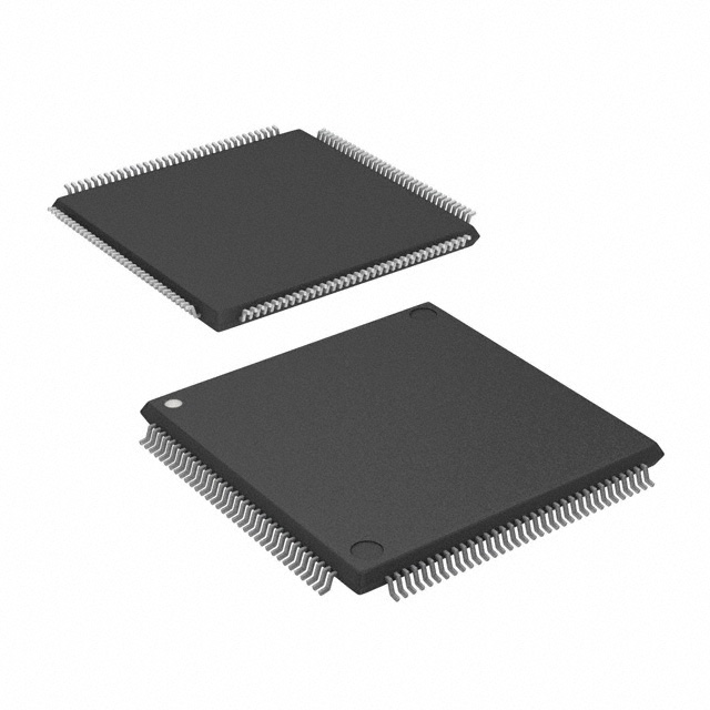
A54SX16A-PQ208M
| Part Description |
SX-A Field Programmable Gate Array (FPGA) IC 175 208-BFQFP |
|---|---|
| Quantity | 64 Available (as of June 15, 2026) |

| Product Category | Field Programmable Gate Array (FPGA) |
|---|---|
| Manufacturer | Microchip Technology |
| Manufacturing Status | Obsolete |
| Manufacturer Standard Lead Time | Contact Us |
| Datasheet |
Specifications & Environmental
| Device Package | 208-PQFP (28x28) | Grade | Military | Operating Temperature | -55°C – 125°C | ||
|---|---|---|---|---|---|---|---|
| Package / Case | 208-BFQFP | Number of I/O | 175 | Voltage | 2.25 V - 5.25 V | ||
| Mounting Method | Surface Mount | RoHS Compliance | RoHS non-compliant | REACH Compliance | REACH Unaffected | ||
| Moisture Sensitivity Level | 3 (168 Hours) | Number of LABs/CLBs | 1452 | Number of Logic Elements/Cells | 1452 | ||
| Number of Gates | 24000 | ECCN | 3A001A2C | HTS Code | 8542.39.0001 | ||
| Qualification | N/A |
Overview of A54SX16A-PQ208M – SX-A Field Programmable Gate Array (FPGA) IC 175 I/O 208-PQFP
The A54SX16A-PQ208M is a military-grade SX-A family FPGA from Microchip Technology optimized for applications requiring nonvolatile, single-chip configurable logic. It provides deterministic timing and in-system diagnostics suitable for high-reliability environments.
This device delivers 24,000 system gates implemented as 1,452 logic elements, up to 175 user-programmable I/O pins, and supports mixed-voltage I/O operation across a wide supply range, making it suitable for secure control, interface and signal-management functions in demanding systems.
Key Features
- Core Performance – Datasheet-rated system and internal performance targets include 250 MHz system performance and up to 350 MHz internal performance for timing-sensitive designs.
- Logic Capacity – 24,000 system gates implemented as approximately 1,452 logic elements, providing a mid-range FPGA fabric for combinational and sequential logic implementations.
- I/O and Interface Flexibility – 175 user I/Os with configurable I/O support for multiple voltage standards; I/Os are hot-swap compliant and power-up/down friendly with no sequencing required for supply voltages.
- Supply Range – Wide voltage supply range from 2.25 V to 5.25 V enabling mixed-voltage system integration and 5 V input tolerance as noted in the SX-A family documentation.
- Nonvolatile Single-Chip Solution – On-chip nonvolatile configuration reduces external components and simplifies board-level design and system startup.
- Package and Mounting – Supplied in a 208-pin PQFP (28 × 28 mm) package intended for surface-mount assembly; package case listed as 208-BFQFP.
- Temperature and Grade – Military temperature grade with an operating range from –55 °C to 125 °C, suitable for harsh environments.
- Reliability and Security Features – Includes boundary-scan (IEEE 1149.1 JTAG) support and Actel Secure Programming Technology with FuseLock™ for protection against reverse engineering, as described in the SX-A family documentation.
- Compliance – RoHS compliant.
- Additional System Features – Family-level features include configurable weak pull-up/pull-down at power-up, individual output slew-rate control, and deterministic, user-controllable timing.
Typical Applications
- Military and Aerospace Systems – Military-grade temperature range (–55 °C to 125 °C) and robust package options support control, signal processing, and interface functions in harsh environments.
- Secure Embedded Control – Nonvolatile single-chip configuration and FuseLock™ programming support secure, field-deployable control and mission-critical logic functions.
- PCI and Interface Logic – SX-A family documentation references 66 MHz PCI compliance and configurable I/O standards, making the device suitable for interface bridging and legacy bus support.
- In-System Verification and Diagnostics – Built-in boundary-scan and in-system diagnostic capabilities simplify board-level test, verification, and field diagnostics workflows.
Unique Advantages
- Deterministic Timing: User-controllable timing and family-documented performance figures help engineers design predictable, timing-sensitive logic.
- Wide Voltage Flexibility: 2.25 V to 5.25 V supply range with mixed-voltage I/O support reduces the need for level-shifting components in mixed-signal systems.
- Nonvolatile Configuration: Single-chip nonvolatile architecture removes external configuration memory, simplifying BOM and improving system reliability during power cycles.
- Military Temperature Rating: Qualified for –55 °C to 125 °C operation, enabling deployment in temperature-extreme applications.
- Security and Testability: FuseLock™ secure programming and IEEE 1149.1 boundary-scan support enhance IP protection and manufacturability.
- Surface-Mount PQFP Packaging: 208-pin PQFP footprint supports high I/O density while maintaining standard surface-mount assembly compatibility.
Why Choose A54SX16A-PQ208M?
The A54SX16A-PQ208M combines the SX-A family’s nonvolatile, deterministic FPGA architecture with a mid-range logic capacity of 24,000 system gates and 1,452 logic elements. Its 175 user I/Os, wide supply voltage window, and military temperature rating make it a fit for secure, reliable designs that must operate across extreme conditions.
Engineers seeking a single-chip, nonvolatile FPGA with built-in security features, boundary-scan testability, and configurable I/O flexibility will find the A54SX16A-PQ208M well suited to rugged embedded and interface applications where long-term robustness and in-system diagnostics are important.
Request a quote or submit an inquiry to obtain pricing, availability, and ordering details for the A54SX16A-PQ208M. Our team can help with lead times and configuration options for your project needs.


Date Founded: 1989
Headquarters: Chandler, Arizona, USA
Employees: 22,000+
Revenue: $8.349 Billion
Certifications and Memberships: ISO9001:2015, IATF16949:2016, AS 9100D


