
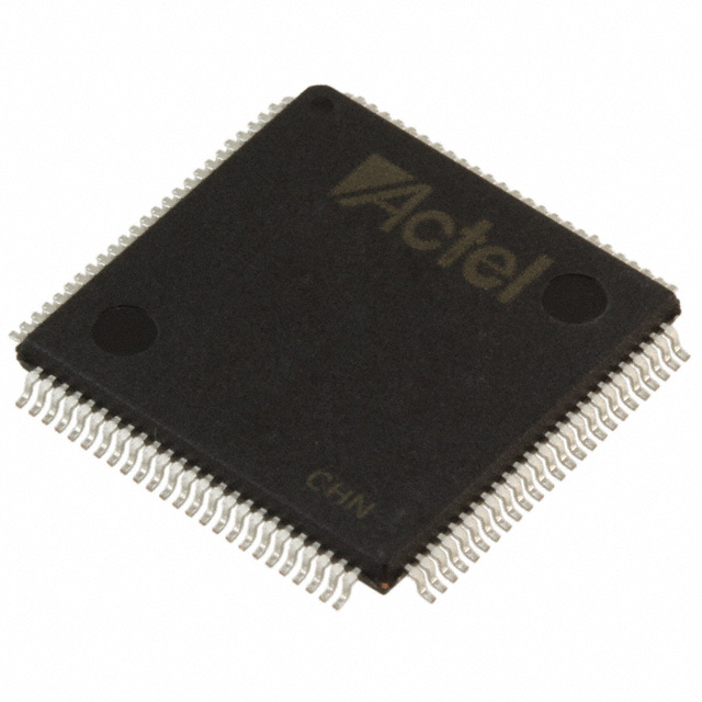
A54SX16A-PQG208M
| Part Description |
SX-A Field Programmable Gate Array (FPGA) IC 175 208-BFQFP |
|---|---|
| Quantity | 1,283 Available (as of June 15, 2026) |

| Product Category | Field Programmable Gate Array (FPGA) |
|---|---|
| Manufacturer | Microchip Technology |
| Manufacturing Status | Active |
| Manufacturer Standard Lead Time | 20 Weeks |
| Datasheet |
Specifications & Environmental
| Device Package | 208-PQFP (28x28) | Grade | Military | Operating Temperature | -55°C – 125°C | ||
|---|---|---|---|---|---|---|---|
| Package / Case | 208-BFQFP | Number of I/O | 175 | Voltage | 2.25 V - 5.25 V | ||
| Mounting Method | Surface Mount | RoHS Compliance | ROHS3 Compliant | REACH Compliance | REACH Unaffected | ||
| Moisture Sensitivity Level | 3 (168 Hours) | Number of LABs/CLBs | 1452 | Number of Logic Elements/Cells | 1452 | ||
| Number of Gates | 24000 | ECCN | 3A001A2C | HTS Code | 8542.39.0001 | ||
| Qualification | N/A |
Overview of A54SX16A-PQG208M – SX-A Field Programmable Gate Array (FPGA) IC 175 208-BFQFP
The A54SX16A-PQG208M is a member of the SX-A family of nonvolatile, single-chip FPGAs from Microchip Technology. This device delivers 24,000 system gates with 1,452 logic elements and 175 user-programmable I/O pins in a 208-pin surface-mount BFQFP package, targeted at applications requiring military-grade temperature and reliability.
Designed for high-reliability embedded systems, the device combines configurable I/O voltage support, deterministic timing, and in-system diagnostic and security capabilities to address applications where rugged performance, secure configuration, and robust I/O handling are required.
Key Features
- Core Performance Family-level performance characteristics include up to 250 MHz system performance and up to 350 MHz internal performance as documented for the SX-A family.
- Logic Resources 24,000 system gates and approximately 1,452 logic elements provide substantial combinatorial and sequential resources for mid-density designs.
- Flip-Flops SX-A family devices support up to 2,012 dedicated flip-flops (family specification).
- I/O Flexibility 175 user I/Os with configurable support for 3.3 V / 5 V PCI, 5 V TTL, 3.3 V LVTTL, and 2.5 V LVCMOS2; 5 V input tolerance and 5 V drive strength are available per family documentation.
- Nonvolatile Single-Chip Configuration Nonvolatile, single-chip architecture eliminates the need for external configuration memory and supports in-system programmability and diagnostics.
- Power and I/O Robustness Hot-swap compliant I/Os and power-up/power-down friendly operation with no sequencing required for supply voltages are included at the family level.
- Security and Test Family features include Actel Secure Programming Technology (FuseLock™) to protect designs and IEEE 1149.1 (JTAG) boundary-scan testing for board-level diagnostics.
- Package and Mounting Surface-mount 208-pin BFQFP (supplier package 208-PQFP, 28×28) for compact board integration.
- Electrical and Environmental Supply voltage range 2.25 V to 5.25 V; RoHS compliant; military grade with operating temperature range of −55 °C to +125 °C.
- On-Chip Memory Total on-chip RAM bits: 0 (no embedded RAM).
Typical Applications
- Military and Aerospace Systems Military-grade temperature range (−55 °C to +125 °C) and surface-mount 208-pin packaging make the device suitable for high-reliability defense and aerospace electronics.
- PCI and Embedded I/O Interfaces Configurable I/O support and family-level 66 MHz PCI compliance enable use in embedded PCI-connected modules and I/O bridging.
- Secure Embedded Control Nonvolatile configuration combined with FuseLock™ security and JTAG boundary-scan supports secure, verifiable field-deployable systems.
- High-Reliability Industrial Electronics Deterministic timing, hot-swap-compliant I/Os, and wide supply voltage tolerance suit rugged industrial control and instrumentation designs.
Unique Advantages
- Military-Grade Operation: Guaranteed operation from −55 °C to +125 °C for applications requiring extreme-temperature reliability.
- Single-Chip Nonvolatile FPGA: Eliminates external configuration memory, reducing BOM complexity and improving system robustness.
- Flexible I/O Voltage Support: Multiple I/O standards and 5 V tolerance simplify integration with mixed-voltage systems and legacy interfaces.
- Built-In Security and Test: FuseLock™ programming protection and IEEE 1149.1 boundary-scan support aid IP protection and board-level testing.
- Compact Surface-Mount Package: 208-pin BFQFP (surface mount) offers a balance of I/O count and PCB space for dense board designs.
- Predictable Timing and Diagnostics: Deterministic timing behavior and in-system diagnostic capabilities help accelerate validation and field troubleshooting.
Why Choose A54SX16A-PQG208M?
The A54SX16A-PQG208M positions itself as a mid-density, military-grade FPGA option within the SX-A family, delivering 24,000 system gates, about 1,452 logic elements, and 175 user I/Os in a compact 208-pin BFQFP package. Its nonvolatile single-chip architecture, combined with configurable I/O and robust power-handling features, makes it well-suited for secure, high-reliability embedded designs where external configuration memory or complex power sequencing is undesirable.
Choose this device for applications that require predictable timing, wide voltage tolerance, and proven family-level features such as JTAG boundary-scan, hot-swap I/O behavior, and configuration security. The combination of military-grade temperature capability and RoHS compliance provides a long-term solution for demanding deployed systems.
Request a quote or submit an inquiry to receive pricing, availability, and technical support information for the A54SX16A-PQG208M.


Date Founded: 1989
Headquarters: Chandler, Arizona, USA
Employees: 22,000+
Revenue: $8.349 Billion
Certifications and Memberships: ISO9001:2015, IATF16949:2016, AS 9100D


