
A54SX16A-TQ100
| Part Description |
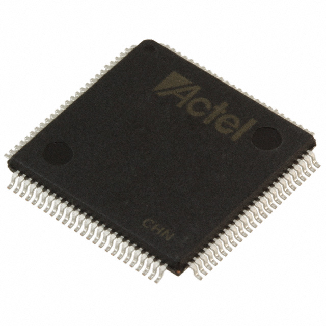
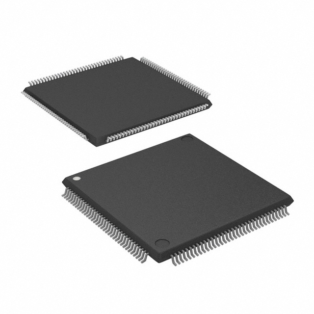
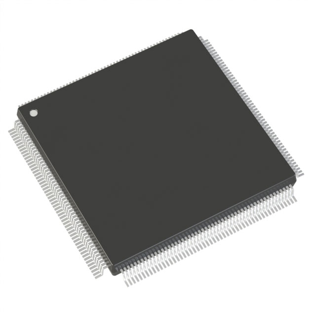
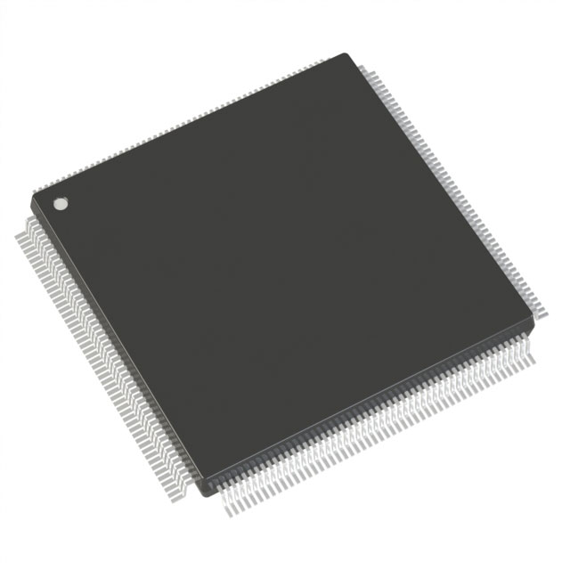
SX-A Field Programmable Gate Array (FPGA) IC 81 100-LQFP |
|---|---|
| Quantity | 816 Available (as of October 8, 2026) |
| Product Category | Field Programmable Gate Array (FPGA) |
|---|---|
| Manufacturer | Microchip Technology |
| Manufacturing Status | Obsolete |
| Manufacturer Standard Lead Time | Contact Us |
| Datasheet |
Specifications & Environmental
| Device Package | 100-TQFP (14x14) | Grade | Commercial | Operating Temperature | 0°C – 70°C | ||
|---|---|---|---|---|---|---|---|
| Package / Case | 100-LQFP | Number of I/O | 81 | Voltage | 2.25 V - 5.25 V | ||
| Mounting Method | Surface Mount | RoHS Compliance | RoHS non-compliant | REACH Compliance | REACH Unaffected | ||
| Moisture Sensitivity Level | 3 (168 Hours) | Number of LABs/CLBs | 1452 | Number of Logic Elements/Cells | 1452 | ||
| Number of Gates | 24000 | ECCN | 3A991D | HTS Code | 8542.39.0001 | ||
| Qualification | N/A |
Overview of A54SX16A-TQ100 – SX-A Field Programmable Gate Array (FPGA) IC 81 100-LQFP
The A54SX16A-TQ100 is a member of the SX-A family of nonvolatile, single-chip FPGAs. It provides 1,452 logic elements (LEs) and 24,000 system gates in a 100-pin thin quad flat pack (TQFP) surface-mount package with 81 user I/Os, targeting commercial embedded designs that require configurable, mixed-voltage I/O and deterministic timing.
Family-level performance characteristics include up to 250 MHz system performance and up to 350 MHz internal performance. The device’s mix of configurable I/O, single-chip nonvolatile configuration and in-system diagnostic features make it suitable for designs that need flexible interfacing, secure programming and board-level testability.
Key Features
- Logic Capacity — 1,452 logic elements and approximately 24,000 system gates provide a compact programmable fabric for mid-range logic integration.
- User I/O — 81 user-programmable I/O pins with configurable I/O standards enabling mixed-voltage operation (2.5 V, 3.3 V, 5 V) and 5 V input tolerance.
- Nonvolatile Single-Chip Configuration — Single-chip, nonvolatile architecture simplifies system design by eliminating the need for external configuration memory.
- Voltage and Power — Wide supply range from 2.25 V to 5.25 V supports mixed-voltage systems and flexible board-level power architectures.
- No On-Chip RAM — Total on-chip RAM bits: 0, for designs that rely on flip-flops and external memory for state storage.
- Performance (Family) — SX-A family-level performance indicators include up to 250 MHz system performance and up to 350 MHz internal performance.
- I/O and System Control — Hot-swap compliant I/Os, configurable weak pull-up/pull-down on power-up, individual output slew rate control and support for PCI signaling options (3.3 V / 5 V PCI).
- Security and Test — Actel Secure Programming Technology with FuseLock™ for protection against reverse engineering and IEEE 1149.1 (JTAG) boundary-scan for board-level test and debug.
- Package and Mounting — 100-pin TQFP (14 × 14 mm) package, surface-mount mounting type, commercial temperature grade (0 °C to +70 °C).
- RoHS Compliance — Device is RoHS compliant for lead-free manufacturing processes.
Typical Applications
- Commercial Embedded Systems — Implement glue logic, custom peripherals and control functions where a compact, nonvolatile FPGA fabric and mixed-voltage I/O are required.
- Board-Level Interface and PCI Peripherals — Support for 3.3 V / 5 V PCI and configurable I/O makes the device suitable for implementing PCI-compliant interfaces and peripheral controllers.
- In-System Test and Diagnostics — JTAG boundary-scan and in-system diagnostic capabilities assist manufacturing test and field verification of board-level interconnects.
- Secure Logic Implementation — FuseLock secure programming technology is useful for designs requiring protection against IP extraction and reverse engineering.
Unique Advantages
- Compact, Mid-Range Integration: 1,452 logic elements and 24,000 system gates provide room for substantial logic consolidation while keeping board space and BOM complexity down.
- Single-Chip Nonvolatile Configuration: Eliminates the need for external configuration memories and simplifies power-up behavior and supply sequencing.
- Flexible Mixed-Voltage I/O: 2.5 V, 3.3 V and 5 V mixed-voltage operation with 5 V tolerance enables direct interfacing to a wide range of legacy and modern peripherals.
- Design Security: FuseLock programming technology provides a hardware-level measure to help prevent reverse engineering of the programmed design.
- Manufacturing and Field Testability: IEEE 1149.1 boundary-scan and in-system diagnostic features support efficient board bring-up and fault isolation.
- Commercial Temperature and RoHS Compliance: Commercial temperature rating (0 °C to +70 °C) and RoHS compliance align the device with standard commercial production environments and regulations.
Why Choose A54SX16A-TQ100?
The A54SX16A-TQ100 delivers a balanced combination of mid-range logic capacity, mixed-voltage I/O flexibility and single-chip nonvolatile configuration in a compact 100-pin TQFP package. Its family-level performance characteristics and built-in security and test features make it appropriate for commercial embedded designs that need deterministic behavior, secure programming and streamlined board-level integration.
This device is well-suited to designers looking to consolidate glue logic, implement PCI-capable interfaces, and accelerate board bring-up with boundary-scan and in-system diagnostics while maintaining a small footprint and RoHS-compliant manufacturing compatibility.
Request a quote or submit a procurement inquiry to receive pricing, availability and delivery details for the A54SX16A-TQ100.





















Date Founded: 1989
Headquarters: Chandler, Arizona, USA
Employees: 22,000+
Revenue: $8.349 Billion
Certifications and Memberships: ISO9001:2015, IATF16949:2016, AS 9100D




