
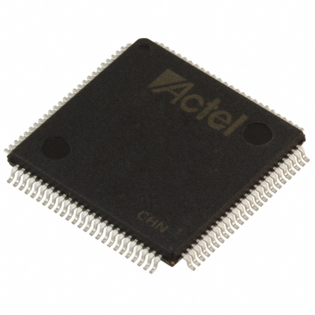
A54SX16A-PQG208I
| Part Description |
SX-A Field Programmable Gate Array (FPGA) IC 175 208-BFQFP |
|---|---|
| Quantity | 819 Available (as of June 14, 2026) |

| Product Category | Field Programmable Gate Array (FPGA) |
|---|---|
| Manufacturer | Microchip Technology |
| Manufacturing Status | Active |
| Manufacturer Standard Lead Time | 14 Weeks |
| Datasheet |
Specifications & Environmental
| Device Package | 208-PQFP (28x28) | Grade | Industrial | Operating Temperature | -40°C – 85°C | ||
|---|---|---|---|---|---|---|---|
| Package / Case | 208-BFQFP | Number of I/O | 175 | Voltage | 2.25 V - 5.25 V | ||
| Mounting Method | Surface Mount | RoHS Compliance | ROHS3 Compliant | REACH Compliance | REACH Unaffected | ||
| Moisture Sensitivity Level | 3 (168 Hours) | Number of LABs/CLBs | 1452 | Number of Logic Elements/Cells | 1452 | ||
| Number of Gates | 24000 | ECCN | 3A991D | HTS Code | 8542.39.0001 | ||
| Qualification | N/A |
Overview of A54SX16A-PQG208I – SX-A Field Programmable Gate Array (FPGA) IC 175 208-BFQFP
The A54SX16A-PQG208I is a member of the SX-A family of nonvolatile, single-chip FPGAs from Microchip Technology. It delivers 24,000 system gates with 1,452 logic elements and up to 175 user I/Os in a 208-pin package, providing reprogrammable logic and flexible I/O for embedded and industrial designs.
Designed for mixed-voltage systems and industrial-temperature operation, this surface-mount FPGA supports a wide supply range (2.25 V to 5.25 V) and operates from –40 °C to 85 °C, making it suitable for PCI-based systems, I/O-intensive controllers, and applications that require secure, in-system programmable logic.
Key Features
- Core Capacity 24,000 system gates and 1,452 logic elements provide programmable logic density for mid-range control, glue-logic, and interface functions.
- User I/O Up to 175 user-programmable I/Os with configurable I/O support for 3.3 V / 5 V PCI, 5 V TTL, 3.3 V LVTTL and 2.5 V LVCMOS2; supports mixed-voltage operation with 5 V input tolerance and 5 V drive strength.
- Performance Family performance targets include system and internal operating frequencies suitable for timing-critical designs (family data lists 250 MHz system and 350 MHz internal performance).
- Nonvolatile Single-Chip Solution Device retains configuration without external memory, simplifying board-level design and eliminating external configuration components.
- Power and I/O Robustness Hot-swap compliant I/Os and power-up/power-down friendly behavior (no supply sequencing required) for reliable integration into live systems.
- Security and Test Actel Secure Programming Technology with FuseLock™ prevents reverse engineering and supports boundary-scan testing compliant with IEEE 1149.1 (JTAG) for board-level testability.
- Package and Mounting 208-BFQFP package case; supplier device package listed as 208-PQFP (28×28). Surface-mount mounting type suitable for standard PCB assembly.
- Environmental and Supply Voltage supply range 2.25 V to 5.25 V, operating temperature –40 °C to 85 °C, and RoHS compliant.
- Timing and Control Deterministic, user-controllable timing features, individual output slew-rate control, and design diagnostic capability for predictable system behavior and in-system verification.
Typical Applications
- PCI and Interface Bridges Use in 66 MHz PCI-compliant systems and I/O bridging where flexible, mixed-voltage I/O and PCI signaling support are required.
- Industrial Control and Automation Reprogrammable logic for motor control, PLC interfacing, and real-time control tasks that benefit from nonvolatile configuration and industrial temperature range.
- System Glue Logic and Protocol Conversion Mid-density logic integration for consolidating discrete components, implementing protocol translation, or adding custom logic functions.
- In-System Diagnostics and Verification Built-in diagnostic capabilities and JTAG boundary-scan support for in-system verification and fault isolation during development and production test.
Unique Advantages
- Nonvolatile, single-chip configuration: Eliminates the need for external configuration memory and simplifies board design.
- Wide supply and mixed-voltage I/O: 2.25 V–5.25 V supply range and multi-standard I/O support reduce the need for level translators and simplify integration with legacy and modern interfaces.
- Industrial temperature rating: Specified operation from –40 °C to 85 °C for reliable field deployment in industrial environments.
- Secure programming and testability: FuseLock security and IEEE 1149.1 boundary-scan support help protect IP and streamline production test.
- Predictable timing control: Deterministic timing features and individual slew-rate control aid in meeting tight system timing and signal integrity requirements.
Why Choose A54SX16A-PQG208I?
The A54SX16A-PQG208I balances mid-range logic density with flexible, mixed-voltage I/Os and industrial-temperature operation to address a broad set of embedded and industrial design challenges. Its nonvolatile single-chip architecture and built-in security and test features reduce BOM complexity while supporting in-system verification and secure programming.
This device is suited for designers who need a robust, reprogrammable logic element that integrates I/O flexibility, deterministic timing, and production-friendly features into a compact 208-pin surface-mount package.
Request a quote or submit a product inquiry to obtain pricing, availability, and support for design integration and volume requirements.


Date Founded: 1989
Headquarters: Chandler, Arizona, USA
Employees: 22,000+
Revenue: $8.349 Billion
Certifications and Memberships: ISO9001:2015, IATF16949:2016, AS 9100D


