
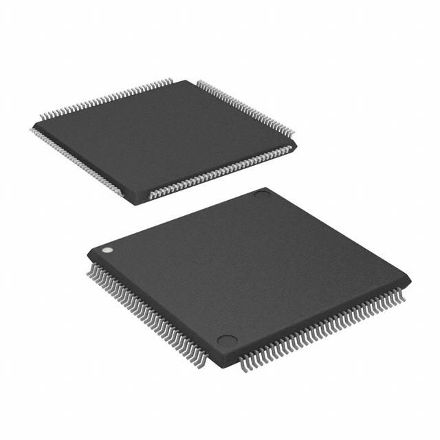
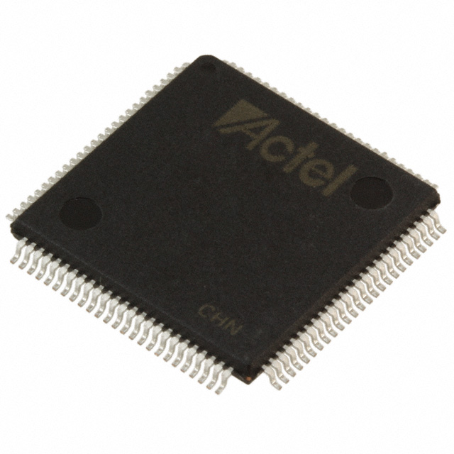
A54SX16A-TQ144M
| Part Description |
SX-A Field Programmable Gate Array (FPGA) IC 113 144-LQFP |
|---|---|
| Quantity | 743 Available (as of June 18, 2026) |

| Product Category | Field Programmable Gate Array (FPGA) |
|---|---|
| Manufacturer | Microchip Technology |
| Manufacturing Status | Obsolete |
| Manufacturer Standard Lead Time | Contact Us |
| Datasheet |
Specifications & Environmental
| Device Package | 144-TQFP (20x20) | Grade | Military | Operating Temperature | -55°C – 125°C | ||
|---|---|---|---|---|---|---|---|
| Package / Case | 144-LQFP | Number of I/O | 113 | Voltage | 2.25 V - 5.25 V | ||
| Mounting Method | Surface Mount | RoHS Compliance | RoHS non-compliant | REACH Compliance | REACH Unaffected | ||
| Moisture Sensitivity Level | 3 (168 Hours) | Number of LABs/CLBs | 1452 | Number of Logic Elements/Cells | 1452 | ||
| Number of Gates | 24000 | ECCN | 3A001A2C | HTS Code | 8542.39.0001 | ||
| Qualification | N/A |
Overview of A54SX16A-TQ144M – SX-A Field Programmable Gate Array (FPGA) 144‑LQFP
The A54SX16A-TQ144M is a military‑grade SX‑A family Field Programmable Gate Array in a 144‑pin quad flat package. It provides approximately 24,000 system gates implemented across 1,452 logic elements and up to 113 user I/Os in the 144‑pin package, targeting designs that require nonvolatile configuration, predictable timing, and operational reliability across a wide temperature range.
Built for applications that need mixed‑voltage I/O support, hot‑swap capability, and in‑system diagnostic features, this single‑chip FPGA delivers family-level performance characteristics including 250 MHz system performance and 350 MHz internal performance.
Key Features
- Logic Capacity — Approximately 24,000 system gates implemented across 1,452 logic elements for moderate complexity digital designs.
- User I/O Count — 113 user‑programmable I/Os in the 144‑pin package, enabling multiple peripheral and interface connections.
- Nonvolatile Single‑Chip Architecture — Single‑chip, nonvolatile configuration removes the need for external configuration memory and supports instant-on behavior.
- Performance — Family specifications list 250 MHz system performance and up to 350 MHz internal performance for timing‑sensitive functions.
- Mixed‑Voltage I/O and 5 V Tolerance — Configurable I/O supports 2.5 V, 3.3 V and 5 V operation with 5 V input tolerance and 5 V drive strength as specified by the SX‑A family features.
- Wide Supply Range — Voltage supply range from 2.25 V to 5.25 V to accommodate diverse system power rails.
- Military Temperature Grade — Operating temperature range −55 °C to 125 °C and specified as Military grade for harsh environments.
- Package and Mounting — 144‑pin LQFP package (supplier package listed as 144‑TQFP 20×20); surface‑mount mounting type.
- System Reliability and Test — Boundary‑scan testing compliant with IEEE 1149.1 (JTAG) and in‑system diagnostic/verification capability as provided in the SX‑A family.
- Security — Family feature: Actel Secure Programming Technology with FuseLock to protect design IP against reverse engineering.
- Power‑Up/Down Friendly — I/Os specified as power‑up/down friendly with no sequencing required for supply voltages in family documentation.
- On‑Chip Memory — Total on‑chip RAM bits: 0, for designs that rely on external memory or register resources.
- RoHS Compliant — Device is RoHS compliant for environmental conformity.
Typical Applications
- PCI Interface Logic — Family‑level PCI compliance and configurable I/O enable implementation of PCI‑related glue logic and interface bridging in systems that require 3.3 V/5 V support.
- Mil‑Grade Control Systems — Military temperature grading (−55 °C to 125 °C) and surface‑mount packaging make the device suitable for deployed defense and avionics electronic control functions.
- In‑System Diagnostics and Verification — Built‑in boundary‑scan and in‑system diagnostic capabilities support board‑level test, field verification, and fault isolation workflows.
- Mixed‑Voltage Interface Bridging — Configurable I/O and wide supply range support mixed‑voltage system interfacing without extensive level‑shifting hardware.
Unique Advantages
- Nonvolatile, single‑chip solution: Eliminates external configuration memory to simplify board layout and reduce BOM count.
- Deterministic timing and high utilization: Family support for deterministic, user‑controllable timing and up to 100% resource utilization helps simplify timing closure and maximize device use.
- Security features: FuseLock secure programming technology protects IP and helps preserve design confidentiality.
- Robust I/O and power handling: Hot‑swap compliant I/Os and power‑up/down friendly behavior reduce system complexity during power sequencing and board hot‑swap events.
- Wide operating conditions: Broad supply range (2.25 V–5.25 V) and military temperature rating support operation across diverse system environments.
- Testability and diagnostics: IEEE 1149.1 boundary‑scan and in‑system diagnostic capabilities speed validation, bring‑up, and field maintenance.
Why Choose A54SX16A-TQ144M?
The A54SX16A-TQ144M positions itself as a reliable, nonvolatile FPGA option for designs needing a moderate logic capacity (approximately 24,000 system gates / 1,452 logic elements) combined with military‑grade environmental performance. Its combination of mixed‑voltage I/O support, hot‑swap compliance, and integrated security and test features make it well suited to applications that demand deterministic behavior, field diagnostics, and IP protection.
This device is appropriate for engineering teams designing mil‑grade control, interface bridging, and diagnostic‑aware systems where long‑term robustness, predictable timing, and simplified board‑level integration are priorities.
If you would like pricing, availability, or a formal quote for the A54SX16A-TQ144M, submit a request or contact sales to arrange a quote or further technical assistance.


Date Founded: 1989
Headquarters: Chandler, Arizona, USA
Employees: 22,000+
Revenue: $8.349 Billion
Certifications and Memberships: ISO9001:2015, IATF16949:2016, AS 9100D


