
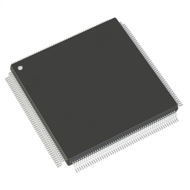
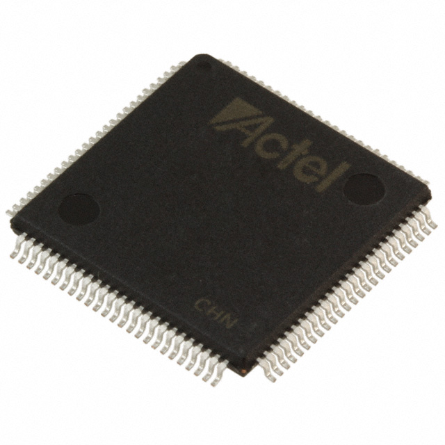
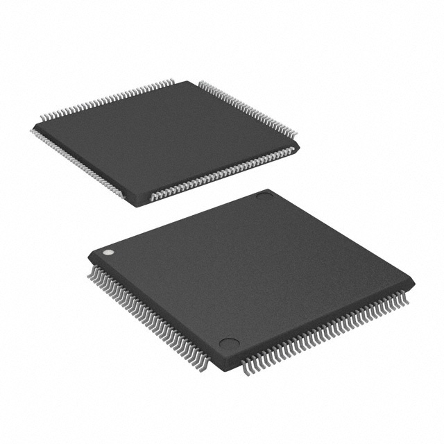
A54SX16A-TQG144A
| Part Description |
SX-A Field Programmable Gate Array (FPGA) IC 113 144-LQFP |
|---|---|
| Quantity | 1,443 Available (as of June 15, 2026) |

| Product Category | Field Programmable Gate Array (FPGA) |
|---|---|
| Manufacturer | Microchip Technology |
| Manufacturing Status | Active |
| Manufacturer Standard Lead Time | 12 Weeks |
| Datasheet |
Specifications & Environmental
| Device Package | 144-TQFP (20x20) | Grade | Automotive | Operating Temperature | -40°C – 125°C | ||
|---|---|---|---|---|---|---|---|
| Package / Case | 144-LQFP | Number of I/O | 113 | Voltage | 2.25 V - 5.25 V | ||
| Mounting Method | Surface Mount | RoHS Compliance | ROHS3 Compliant | REACH Compliance | REACH Unaffected | ||
| Moisture Sensitivity Level | 3 (168 Hours) | Number of LABs/CLBs | 1452 | Number of Logic Elements/Cells | 1452 | ||
| Number of Gates | 24000 | ECCN | 3A991D | HTS Code | 8542.39.0001 | ||
| Qualification | AEC-Q100 |
Overview of A54SX16A-TQG144A – SX-A Field Programmable Gate Array (FPGA) IC 113 144-LQFP
The A54SX16A-TQG144A is a nonvolatile SX-A family FPGA offered in a 144-pin TQFP/LQFP package with 24,000 system gates and 1,452 logic elements. Designed and qualified to AEC-Q100 automotive standards, it provides deterministic, user-controllable timing and configurable I/O, making it suitable for embedded control and interface functions within temperature-critical environments.
Core advantages include a broad supply voltage range (2.25 V to 5.25 V), 113 user I/Os, and family-level features such as hot-swap compliant I/Os, boundary-scan (JTAG) support, and secure programming technology.
Key Features
- Core Capacity — 24,000 system gates with 1,452 logic elements, supporting medium-complexity FPGA designs.
- I/O and Interfaces — 113 user I/Os on the 144-pin package with configurable I/O standards and individual output slew rate control for interface flexibility.
- Nonvolatile Architecture — Nonvolatile configuration preserves design state across power cycles, removing the need for external configuration memory.
- Automotive Qualification — AEC-Q100 qualification and an operating temperature range of −40°C to 125°C for automotive-grade deployment.
- Power and Supply — Wide supply voltage support from 2.25 V to 5.25 V and power-up/down friendly behavior with no supply sequencing required.
- Performance and Timing — Family-level internal performance up to 250 MHz and deterministic, user-controllable timing for predictable system behavior.
- System Reliability — Boundary-scan testing (IEEE 1149.1) and Actel Secure Programming Technology (FuseLock™) to protect designs and support testability.
- Package and Mounting — Available in a 144-LQFP / 144-TQFP (20 × 20) plastic package, surface-mount compatible for standard PCB assembly flows.
- Standards and Compliance — RoHS compliant and PCI-capable at the family level (66 MHz PCI support noted in family datasheet).
Typical Applications
- Automotive Control Systems — Automotive-grade qualification and extended temperature range enable deployment in electronic control units and sensor interface modules.
- In-vehicle Interfaces — Configurable I/O standards and 113 user-accessible I/Os support protocol bridging and custom vehicle interface logic.
- Hot-swap and Power-sensitive Designs — Hot-swap compliant I/Os and power-up/down friendly behavior simplify systems that require live insertion or multiple supply domains.
Unique Advantages
- Automotive-Grade Qualification: AEC-Q100 qualification and −40°C to 125°C operating range reduce validation effort for automotive applications.
- Nonvolatile Configuration: Built-in nonvolatile architecture eliminates the need for external configuration memory, reducing BOM and simplifying startup.
- Secure Programming: FuseLock™ secure programming protects intellectual property and prevents reverse engineering of the programmed bitstream.
- Flexible I/O and Timing: Configurable I/O standards, individual slew-rate control, and deterministic timing provide interface flexibility and predictable system behavior.
- Test and Debug Support: Boundary-scan (IEEE 1149.1) and in-system diagnostic capabilities improve board-level testability and development visibility.
Why Choose A54SX16A-TQG144A?
The A54SX16A-TQG144A positions itself as a robust, automotive-qualified FPGA option for medium-complexity embedded designs that require nonvolatile configuration, predictable timing, and flexible I/O. With 24,000 system gates, 1,452 logic elements and 113 user I/Os in a 144-pin surface-mount package, it balances integration and interface capability for control, interface, and power-sensitive systems.
It is suited to engineering teams seeking an FPGA with automotive qualification, secure programming, and family-proven features such as hot-swap I/Os and boundary-scan testability—providing scalability and long-term reliability for production deployments.
Request a quote or submit a pricing inquiry to evaluate the A54SX16A-TQG144A for your next design.


Date Founded: 1989
Headquarters: Chandler, Arizona, USA
Employees: 22,000+
Revenue: $8.349 Billion
Certifications and Memberships: ISO9001:2015, IATF16949:2016, AS 9100D


