
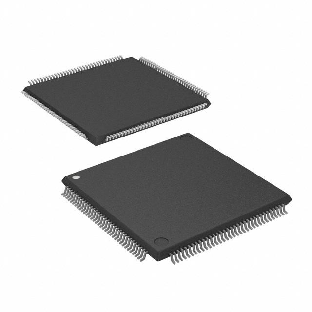
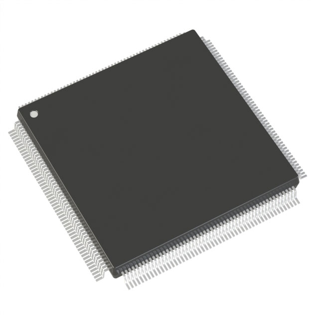
A54SX32-1PQ208M
| Part Description |
SX Field Programmable Gate Array (FPGA) IC 174 208-BFQFP |
|---|---|
| Quantity | 1,211 Available (as of June 15, 2026) |

| Product Category | Field Programmable Gate Array (FPGA) |
|---|---|
| Manufacturer | Microchip Technology |
| Manufacturing Status | Obsolete |
| Manufacturer Standard Lead Time | Contact Us |
| Datasheet |
Specifications & Environmental
| Device Package | 208-PQFP (28x28) | Grade | Military | Operating Temperature | -55°C – 125°C | ||
|---|---|---|---|---|---|---|---|
| Package / Case | 208-BFQFP | Number of I/O | 174 | Voltage | 3 V - 5.5 V | ||
| Mounting Method | Surface Mount | RoHS Compliance | RoHS non-compliant | REACH Compliance | REACH Unaffected | ||
| Moisture Sensitivity Level | 3 (168 Hours) | Number of LABs/CLBs | 2880 | Number of Logic Elements/Cells | 2880 | ||
| Number of Gates | 48000 | ECCN | 3A001A2C | HTS Code | 8542.39.0001 | ||
| Qualification | N/A |
Overview of A54SX32-1PQ208M – SX Field Programmable Gate Array (FPGA) IC 174 208-BFQFP
The A54SX32-1PQ208M is a military-grade SX family Field Programmable Gate Array (FPGA) provided in a 208-pin BFQFP package. It delivers a nonvolatile, single-chip FPGA solution with 48,000 system gates and 2,880 logic elements for control, interfacing and custom digital logic integration.
Key engineering attributes include 174 user I/Os, wide supply voltage support from 3 V to 5.5 V, and an extended operating temperature range from −55 °C to 125 °C, making the device suitable for high-reliability and harsh-environment electronics requiring reconfigurable logic and robust I/O options.
Key Features
- Logic Capacity — 48,000 system gates and 2,880 logic elements provide a mid-range density for implementing custom logic, control and interface functions.
- I/O Count and Flexibility — 174 user-programmable I/Os with configurable I/O support for 3.3 V / 5 V PCI, 5 V TTL, 3.3 V LVTTL and 2.5 V LVCMOS2, plus 5 V input tolerance and 5 V drive strength options.
- Performance — Series datasheet specifies up to 250 MHz system performance and up to 350 MHz internal performance for timing-critical logic paths.
- Nonvolatile Single-Chip Architecture — On-chip nonvolatile configuration removes the need for external configuration memory and supports power-up/power-down-friendly operation without sequencing requirements.
- System and Test Support — Boundary-scan testing compliant with IEEE 1149.1 (JTAG) and in-system diagnostic/verification capability via Silicon Explorer II.
- Power and I/O Controls — Hot-swap compliant I/Os, configurable weak pull-up/pull-down at power-up, and individual output slew-rate control for signal integrity and board-level flexibility.
- Security and Resource Control — Actel Secure Programming Technology with FuseLock™ for protection of device programming and 100% resource utilization with 100% pin locking for deterministic mapping.
- Package and Mounting — 208-BFQFP package case (supplier device package: 208-PQFP 28×28) with surface-mount construction appropriate for standard PCB assembly.
- Environmental Grade — Military grade device with operating temperature range of −55 °C to 125 °C.
- Supply Voltage Range — Operates from 3 V to 5.5 V to support mixed-voltage system environments.
- On-Chip Memory — No embedded RAM (total on-chip RAM bits: 0).
Typical Applications
- PCI-based systems — The device’s 66 MHz PCI compliance and multi-voltage I/O support make it suitable for board-level PCI interface logic and bridging.
- Military and high-reliability electronics — Military grade temperature range and surface-mount packaging suit rugged, mission-critical control and signal-processing applications.
- Mixed-voltage interface control — Configurable I/Os and 5 V tolerance enable protocol translation and glue-logic between different voltage domains on complex PCBs.
- Test and verification environments — Boundary-scan (IEEE 1149.1) and in-system diagnostics facilitate manufacturing test, board bring-up and field verification.
Unique Advantages
- Wide operating temperature range: −55 °C to 125 °C supports deployment in extreme and military environments where thermal resilience is required.
- Nonvolatile configuration: Single-chip nonvolatile architecture eliminates external configuration memory, simplifying BOM and boot behavior.
- Flexible voltage interoperability: Native support for multiple I/O standards (PCI/TTL/LVTTL/LVCMOS2) and mixed-voltage operation reduces the need for intermediate level-shifting components.
- Deterministic timing and full resource control: 100% resource utilization and pin locking enable predictable placement and timing for safety- and performance-conscious designs.
- Built-in security and testability: FuseLock programming protection and JTAG boundary-scan provide anti-tamper measures and streamlined test integration.
- Mid-range density with high I/O count: 48,000 gates and 174 user I/Os provide a balance of logic capacity and connectivity for complex control and interface tasks.
Why Choose A54SX32-1PQ208M?
The A54SX32-1PQ208M positions itself as a resilient, nonvolatile FPGA option for applications that require mid-range logic capacity, extensive I/O flexibility and a military-grade operating window. Its combination of 48,000 system gates, 2,880 logic elements and 174 configurable I/Os addresses board-level interface, control and glue-logic use cases while reducing external configuration components.
Engineers selecting this device benefit from deterministic timing, rugged temperature performance and integrated security/test features — attributes that support long-term reliability, simplified assembly and streamlined test flows in demanding system designs.
Request a quote or submit an inquiry to receive pricing and availability information for the A54SX32-1PQ208M.


Date Founded: 1989
Headquarters: Chandler, Arizona, USA
Employees: 22,000+
Revenue: $8.349 Billion
Certifications and Memberships: ISO9001:2015, IATF16949:2016, AS 9100D


