
A54SX32-1PQG208I
| Part Description |
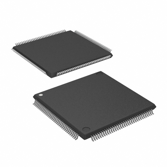
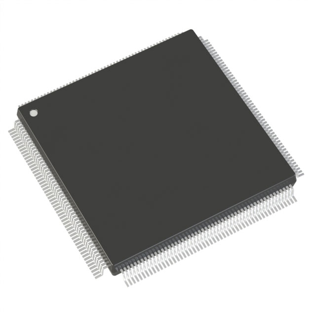
SX Field Programmable Gate Array (FPGA) IC 174 208-BFQFP |
|---|---|
| Quantity | 1,428 Available (as of June 18, 2026) |

| Product Category | Field Programmable Gate Array (FPGA) |
|---|---|
| Manufacturer | Microchip Technology |
| Manufacturing Status | Active |
| Manufacturer Standard Lead Time | 14 Weeks |
| Datasheet |
Specifications & Environmental
| Device Package | 208-PQFP (28x28) | Grade | Industrial | Operating Temperature | -40°C – 85°C | ||
|---|---|---|---|---|---|---|---|
| Package / Case | 208-BFQFP | Number of I/O | 174 | Voltage | 3 V - 5.5 V | ||
| Mounting Method | Surface Mount | RoHS Compliance | ROHS3 Compliant | REACH Compliance | REACH Unaffected | ||
| Moisture Sensitivity Level | 3 (168 Hours) | Number of LABs/CLBs | 2880 | Number of Logic Elements/Cells | 2880 | ||
| Number of Gates | 48000 | ECCN | 3A991D | HTS Code | 8542.39.0001 | ||
| Qualification | N/A |
Overview of A54SX32-1PQG208I – SX Field Programmable Gate Array (FPGA) IC 174 208-BFQFP
The A54SX32-1PQG208I is a nonvolatile SX-A family FPGA from Microchip Technology designed for industrial embedded applications. It integrates approximately 48,000 system gates and 2,880 logic elements with up to 174 user-programmable I/O pins in a 208-pin surface-mount PQFP package.
This device targets designs that require mixed-voltage I/O flexibility, deterministic timing control, and secure, in-system programmability across an industrial temperature range of –40°C to 85°C and a supply range of 3.0 V to 5.5 V.
Key Features
- Core Capacity Approximately 48,000 system gates and 2,880 logic elements provide a mid-range FPGA resource set for control, glue-logic and interface tasks.
- Performance SX-A family performance characteristics include up to 250 MHz system performance and 350 MHz internal performance as documented for the family.
- User I/O Up to 174 user-programmable I/Os in the 208-pin PQFP package with configurable I/O support for multiple voltage standards and 5 V input tolerance.
- Mixed-Voltage Operation Supports 2.5 V, 3.3 V, and 5 V mixed-voltage operation with configurable I/O levels including 5 V TTL, 3.3 V LVTTL, and 2.5 V LVCMOS2.
- Power and Reliability Power-up/down friendly design with no supply-sequencing required and hot-swap compliant I/Os to simplify system power management.
- Security and Test Actel Secure Programming Technology (FuseLock™) for protection against reverse engineering, plus IEEE 1149.1 JTAG boundary-scan testing support.
- Deterministic Timing & Utilization Deterministic, user-controllable timing with up to 100% resource utilization and 100% pin locking for predictable implementation.
- Package & Environmental 208-pin BFQFP (PQFP 28×28) surface-mount package, RoHS compliant, industrial temperature grade (–40°C to 85°C).
- Supply Voltage Operates from 3.0 V to 5.5 V to accommodate a wide range of system power domains.
Typical Applications
- Industrial Control Implement machine-control, sequencing and interface logic where industrial temperature operation (–40°C to 85°C) and mixed-voltage interfacing are required.
- Interface Bridging & Glue Logic Use the device’s 174 I/Os and configurable voltage support to bridge between 2.5 V, 3.3 V and 5 V domains and consolidate discrete logic.
- Secure Embedded Systems Leverage FuseLock secure programming and in-system diagnostic capability (Silicon Explorer II support documented for the family) for protected firmware/bitstream deployment and verification.
- PCI and Legacy Bus Integration Family-level compliance notes include 66 MHz PCI capability and configurable I/O to support legacy bus interfaces.
Unique Advantages
- Nonvolatile single-chip solution: Eliminates the need for external configuration memory, simplifying system design.
- Flexible mixed-voltage I/O: Configurable I/O standards and 5 V tolerance enable straightforward interfacing with a variety of peripherals and legacy logic.
- Industrial-ready thermal range: Rated for –40°C to 85°C to meet industrial deployment requirements.
- Secure programming and test support: FuseLock™ programming and IEEE 1149.1 boundary-scan enable both IP protection and manufacturing testability.
- Deterministic timing and high utilization: User-controllable timing and up to 100% resource utilization help achieve predictable performance in constrained designs.
- RoHS compliant packaging: Meets lead-free environmental requirements for modern electronics manufacturing.
Why Choose A54SX32-1PQG208I?
The A54SX32-1PQG208I offers a balanced combination of mid-range logic capacity, substantial I/O count, and industrial-grade environmental performance for developers building embedded control, interface, and secure systems. Its family-provided performance characteristics and mixed-voltage I/O support make it well-suited for applications that require deterministic timing, nonvolatile configuration, and hardware-level security.
With RoHS compliance, surface-mount PQFP packaging, and secure in-system programmability, this device provides a compact, integrable platform for designs that require reliable operation across a broad supply range (3.0 V–5.5 V) and industrial temperatures.
Request a quote or submit an inquiry to receive pricing and availability for the A54SX32-1PQG208I.


Date Founded: 1989
Headquarters: Chandler, Arizona, USA
Employees: 22,000+
Revenue: $8.349 Billion
Certifications and Memberships: ISO9001:2015, IATF16949:2016, AS 9100D


