
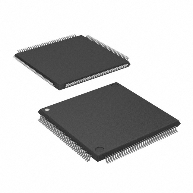
A54SX32-TQ144M
| Part Description |
SX Field Programmable Gate Array (FPGA) IC 113 144-LQFP |
|---|---|
| Quantity | 521 Available (as of October 8, 2026) |
| Product Category | Field Programmable Gate Array (FPGA) |
|---|---|
| Manufacturer | Microchip Technology |
| Manufacturing Status | Obsolete |
| Manufacturer Standard Lead Time | Contact Us |
| Datasheet |
Specifications & Environmental
| Device Package | 144-TQFP (20x20) | Grade | Military | Operating Temperature | -55°C – 125°C | ||
|---|---|---|---|---|---|---|---|
| Package / Case | 144-LQFP | Number of I/O | 113 | Voltage | 3 V - 5.5 V | ||
| Mounting Method | Surface Mount | RoHS Compliance | RoHS non-compliant | REACH Compliance | REACH Unaffected | ||
| Moisture Sensitivity Level | 3 (168 Hours) | Number of LABs/CLBs | 2880 | Number of Logic Elements/Cells | 2880 | ||
| Number of Gates | 48000 | ECCN | 3A001A2C | HTS Code | 8542.39.0001 | ||
| Qualification | N/A |
Overview of A54SX32-TQ144M – SX Field Programmable Gate Array (FPGA) IC 113 144-LQFP
The A54SX32-TQ144M is a military-grade SX family FPGA from Microchip Technology provided in a 144-pin quad flat package. It combines a nonvolatile, single-chip FPGA architecture with 48,000 system gates and 2,880 logic elements to support control, signal processing and glue-logic functions in systems that require wide temperature range operation and 5 V-tolerant I/O.
Designed for applications that demand robust environmental performance, the device supports mixed-voltage operation and configurable I/O, and benefits from SX-A family design characteristics such as high internal performance and in-system diagnostic capability.
Key Features
- Logic Capacity Approximately 48,000 system gates realized through 2,880 logic elements, enabling medium-density FPGA implementations.
- User I/O 113 user-programmable I/O pins with configurable I/O support across 2.5 V, 3.3 V and 5 V signaling levels and 5 V input tolerance (SX-A family capability).
- Performance (Family) SX-A family performance characteristics include up to 250 MHz system performance and up to 350 MHz internal performance as described for the family.
- Nonvolatile, Single-Chip Solution SX-A family devices are provided as nonvolatile, single-chip FPGAs, simplifying configuration and system-level design.
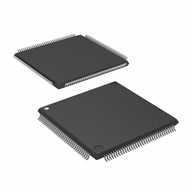
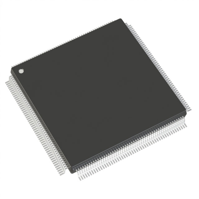
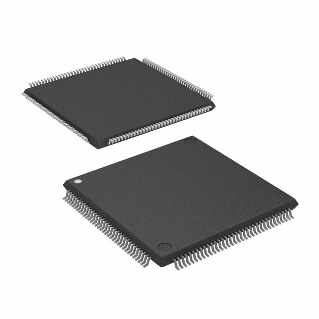
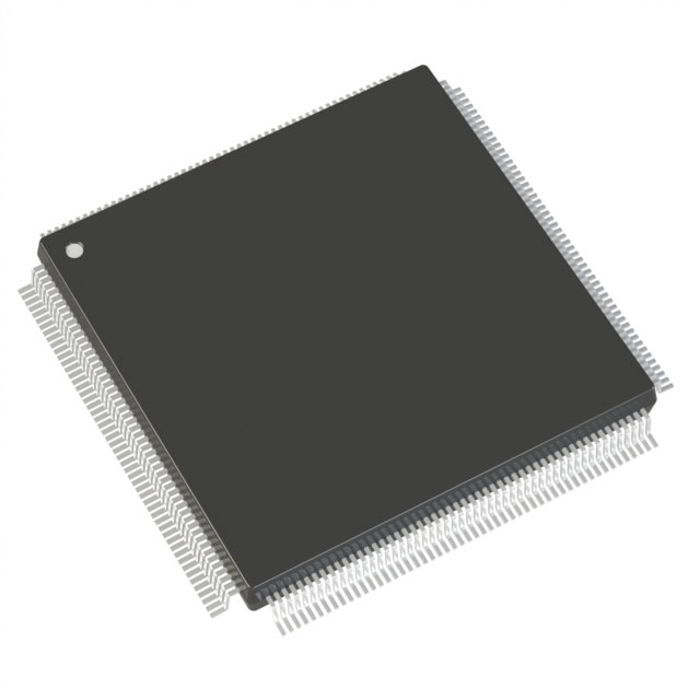
- Package and Mounting 144-pin LQFP package case with supplier package listed as 144-TQFP (20 × 20 mm); surface-mount mounting type.
- Power Wide supply-voltage support from 3 V to 5.5 V to accommodate mixed-voltage systems and legacy interfaces.
- Temperature and Grade Military grade part with operating temperature range from −55 °C to 125 °C for use in demanding environments.
- On-chip Memory Total on-chip RAM bits: 0 (architecture oriented around logic elements and flip‑flops).
- Family Features SX-A family features include hot-swap compliant I/Os, power-up/power-down friendly operation (no sequencing required for supply voltages), boundary-scan testing (IEEE 1149.1), and in-system diagnostic/verification capability.
Typical Applications
- Military and Aerospace Systems Military-grade temperature range and package make the device suitable for ruggedized control, interface conversion and custom logic in defense and aerospace electronics.
- Embedded System Glue Logic Use as mid-density programmable logic to consolidate interface translation, protocol bridging and board-level control functions with configurable I/O voltages.
- In-System Diagnostics and Test Leverage SX-A family boundary-scan and in-system diagnostic capabilities for production testability and field verification.
- Legacy Interface Support Mixed-voltage I/O and 5 V tolerance support integration with legacy 5 V TTL/PCI interfaces where required.
Unique Advantages
- Military-Grade Reliability: Rated for −55 °C to 125 °C operation to meet stringent environmental requirements.
- Flexible I/O Voltage Support: Configurable I/O and mixed-voltage operation provide straightforward interfacing to 2.5 V, 3.3 V and 5 V subsystems.
- Nonvolatile Single-Chip FPGA: No external configuration memory required—simplifies BOM and board-level design.
- Deterministic, In-System Testability: Boundary-scan and diagnostic features from the SX-A family support manufacturing test and in-field verification.
- Wide Supply Range: 3 V to 5.5 V supply range accommodates diverse system architectures and legacy power domains.
Why Choose A54SX32-TQ144M?
The A54SX32-TQ144M positions itself as a robust, nonvolatile FPGA option for designs requiring medium logic density, configurable multi-voltage I/O and military-grade environmental performance. Its balance of 48,000 system gates and approximately 2,880 logic elements makes it suitable for consolidating control and interface functions while retaining deterministic behavior and testability from the SX-A family.
Backed by Microchip Technology’s SX-A family design characteristics, the device is appropriate for engineers developing resilient systems that must operate across wide temperature ranges and interface with mixed-voltage subsystems, offering an upgrade path within the SX family for varying capacity and package needs.
Request a quote or submit a product inquiry to obtain pricing, availability and additional ordering information for the A54SX32-TQ144M.





















Date Founded: 1989
Headquarters: Chandler, Arizona, USA
Employees: 22,000+
Revenue: $8.349 Billion
Certifications and Memberships: ISO9001:2015, IATF16949:2016, AS 9100D




