
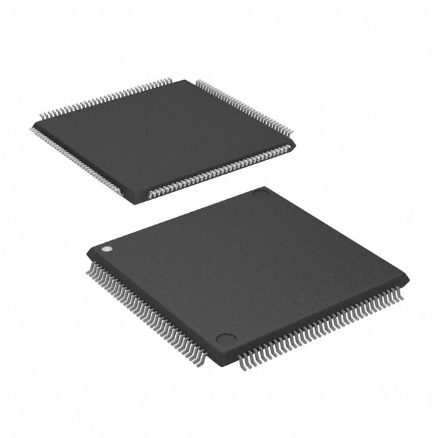
A54SX32-TQG144M
| Part Description |
SX Field Programmable Gate Array (FPGA) IC 113 144-LQFP |
|---|---|
| Quantity | 1,564 Available (as of June 15, 2026) |

| Product Category | Field Programmable Gate Array (FPGA) |
|---|---|
| Manufacturer | Microchip Technology |
| Manufacturing Status | Active |
| Manufacturer Standard Lead Time | 20 Weeks |
| Datasheet |
Specifications & Environmental
| Device Package | 144-TQFP (20x20) | Grade | Military | Operating Temperature | -55°C – 125°C | ||
|---|---|---|---|---|---|---|---|
| Package / Case | 144-LQFP | Number of I/O | 113 | Voltage | 3 V - 5.5 V | ||
| Mounting Method | Surface Mount | RoHS Compliance | ROHS3 Compliant | REACH Compliance | REACH Unaffected | ||
| Moisture Sensitivity Level | 3 (168 Hours) | Number of LABs/CLBs | 2880 | Number of Logic Elements/Cells | 2880 | ||
| Number of Gates | 48000 | ECCN | 3A001A2C | HTS Code | 8542.39.0001 | ||
| Qualification | N/A |
Overview of A54SX32-TQG144M – SX Field Programmable Gate Array (FPGA) IC 113 144-LQFP
The A54SX32-TQG144M is a military-grade SX-A family field programmable gate array (FPGA) offered in a 144-pin thin quad flat pack / LQFP footprint. It delivers a nonvolatile, single-chip FPGA architecture targeted at applications requiring rugged temperature performance and flexible mixed-voltage I/O.
With approximately 48,000 system gates, 2,880 logic elements and 113 user I/Os, the device is suitable for designs that need deterministic timing, in-system diagnostics and configurable I/O support across common interface voltage standards.
Key Features
- Core capacity Approximately 48,000 system gates and 2,880 logic elements, supporting designs with medium logic density requirements.
- User I/O 113 user-programmable I/O pins with configurable weak pull-up/pull-down and individual output slew control for interface flexibility.
- Performance SX-A family performance characteristics include up to 250 MHz system performance and up to 350 MHz internal performance.
- Nonvolatile single-chip solution On-chip nonvolatile configuration removes the need for separate configuration memory and supports power-up/power-down friendly operation.
- Mixed-voltage and 5 V tolerance Configurable I/O support for 3.3 V / 5 V PCI, 5 V TTL, 3.3 V LVTTL and 2.5 V LVCMOS2, enabling mixed-voltage system designs.
- System integration and test Boundary-scan testing compliant with IEEE 1149.1 (JTAG) and in-system diagnostic/verification capability with Silicon Explorer II.
- Security Actel Secure Programming Technology with FuseLock™ to protect design IP and prevent reverse engineering.
- Package and mounting 144-LQFP / supplier 144-TQFP (20 × 20 mm) package, surface-mount mounting type; RoHS compliant.
- Rugged temperature range Designed for military temperature grade operation from −55 °C to 125 °C.
- Voltage supply Operates from 3 V to 5.5 V to accommodate a range of system power rails.
Typical Applications
- Military and aerospace control Suitable for control and signal-processing functions that require military-grade temperature performance and RoHS compliance.
- Mixed-voltage interface bridging Used to implement protocol translation and interface logic where 5 V and 3.3 V signalling coexist, leveraging the configurable I/O and 5 V tolerance.
- Deterministic logic and timing subsystems Applicable where predictable timing and in-system diagnostics (JTAG, Silicon Explorer II) are required for validation and fault isolation.
- Nonvolatile programmable logic Ideal for systems that benefit from a single-chip, nonvolatile FPGA solution to avoid external configuration memory and simplify power-up behavior.
Unique Advantages
- Military-grade thermal resilience: Rated for −55 °C to 125 °C to meet demanding environmental requirements.
- Nonvolatile single-chip architecture: Eliminates separate configuration memory, simplifying board-level design and power sequencing.
- Flexible mixed-voltage I/O: Configurable support for multiple I/O standards and 5 V tolerance eases integration with legacy and modern logic families.
- On-board security features: FuseLock™ secure programming protects design IP and helps prevent reverse engineering.
- Deterministic performance and diagnostics: Documented system and internal performance figures plus JTAG and in-system diagnostic capabilities speed development and validation.
- Compact, surface-mount packaging: 144-LQFP / 144-TQFP (20 × 20) enables high-density PCB layouts while maintaining ample I/O count.
Why Choose A54SX32-TQG144M?
The A54SX32-TQG144M combines a nonvolatile SX-A family FPGA architecture with a mid-range logic capacity of roughly 48,000 system gates and 2,880 logic elements, making it a practical choice for embedded designs that require mixed-voltage interfacing, deterministic timing and military-temperature operation. Its configurable I/O and on-chip security features help reduce system complexity while protecting intellectual property.
This part is well suited to engineers designing rugged, compact systems that need a single-chip programmable logic solution with established diagnostic and boundary-scan support. The combination of RoHS compliance, surface-mount 144-pin packaging and broad supply voltage range supports a variety of board-level implementations.
If you would like pricing, availability or a formal quote for the A54SX32-TQG144M, submit a request or contact sales to receive more information and assistance with ordering.


Date Founded: 1989
Headquarters: Chandler, Arizona, USA
Employees: 22,000+
Revenue: $8.349 Billion
Certifications and Memberships: ISO9001:2015, IATF16949:2016, AS 9100D


