
A54SX32A-1BG329M
| Part Description |
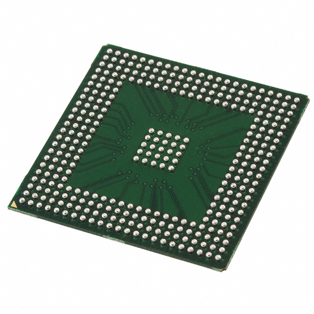
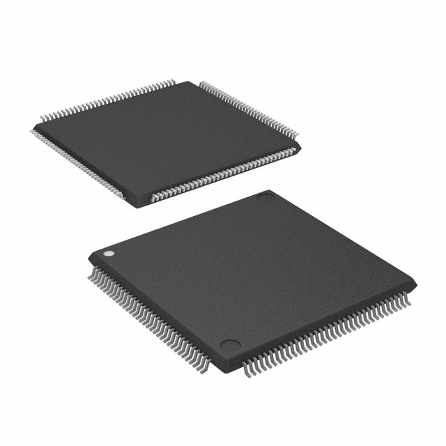
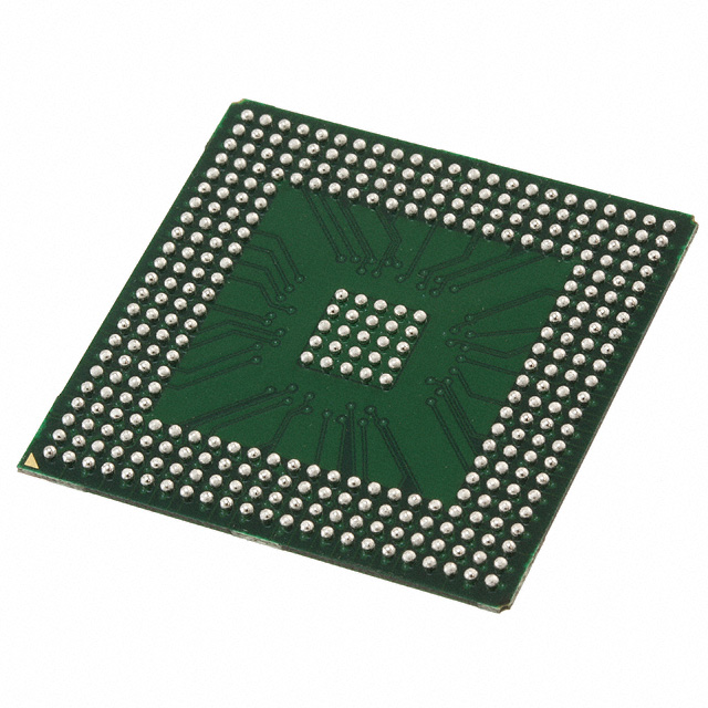
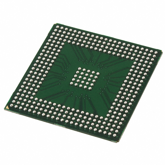
SX-A Field Programmable Gate Array (FPGA) IC 249 329-BBGA |
|---|---|
| Quantity | 695 Available (as of October 8, 2026) |
| Product Category | Field Programmable Gate Array (FPGA) |
|---|---|
| Manufacturer | Microchip Technology |
| Manufacturing Status | Active |
| Manufacturer Standard Lead Time | 20 Weeks |
| Datasheet |
Specifications & Environmental
| Device Package | 329-PBGA (31x31) | Grade | Military | Operating Temperature | -55°C – 125°C | ||
|---|---|---|---|---|---|---|---|
| Package / Case | 329-BBGA | Number of I/O | 249 | Voltage | 2.25 V - 5.25 V | ||
| Mounting Method | Surface Mount | RoHS Compliance | RoHS non-compliant | REACH Compliance | REACH Unaffected | ||
| Moisture Sensitivity Level | 3 (168 Hours) | Number of LABs/CLBs | 2880 | Number of Logic Elements/Cells | 2880 | ||
| Number of Gates | 48000 | ECCN | 3A001A2C | HTS Code | 8542.39.0001 | ||
| Qualification | N/A |
Overview of A54SX32A-1BG329M – SX-A Field Programmable Gate Array (FPGA), 249 I/O, 329-BBGA
The A54SX32A-1BG329M is a nonvolatile SX-A family FPGA in a 329-ball PBGA package, designed for applications requiring a high I/O count and military temperature capability. This device provides 48,000 system gates implemented as approximately 2,880 logic elements and supports mixed-voltage I/O and in-system diagnostics.
With support for wide voltage operation and MIL-grade temperature range, the A54SX32A-1BG329M targets defense, high-reliability industrial, and communications designs that need deterministic timing, secure configuration, and a high-density I/O footprint.
Key Features
- Core Capacity — 48,000 system gates implemented as 2,880 logic elements (combinatorial cells and register resources).
- I/O Density — 249 user-programmable I/O pins to support complex I/O interfacing and multi-channel systems.
- Nonvolatile Single-Chip Solution — Single-chip, nonvolatile architecture for persistent configuration without external memory.
- Performance — Documented family-level performance points include up to 250 MHz system performance and up to 350 MHz internal performance.
- Configurable I/O and Mixed-Voltage Support — Configurable I/O for 3.3 V / 5 V PCI, 5 V TTL, 3.3 V LVTTL, 2.5 V LVCMOS2 and support for 2.5 V, 3.3 V, and 5 V mixed-voltage operation with 5 V input tolerance.
- Power and Supply — Device operates from a 2.25 V to 5.25 V supply range; power-up/down friendly with no required sequencing of supply voltages.
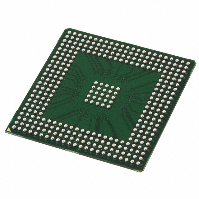
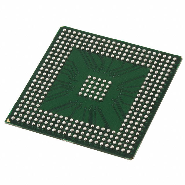
- Package and Mounting — 329-BBGA package (supplier device package: 329-PBGA, 31×31) in a surface-mount form factor for compact, high-density board designs.
- Thermal and Grade — Military-grade device with an operating temperature range of −55 °C to 125 °C for deployment in harsh environments.
- System Reliability and Security — Includes boundary-scan testing (IEEE 1149.1/JTAG) and secure programming technology (FuseLock™) to protect designs against reverse engineering.
- In-System Diagnostics — Family-level support for in-system diagnostic and verification capabilities to aid board bring-up and debug.
- RoHS Compliance — Device is RoHS compliant for environmental conformity.
- On-Chip Memory — Total on-chip RAM: 0 bits (no embedded RAM).
Typical Applications
- Military and Defense Electronics — Military-grade temperature range and robust packaging make the device suitable for ruggedized control and interface functions in defense systems.
- High-Reliability Industrial Control — High I/O count and mixed-voltage support enable sensor interfacing, motor control, and system glue logic in industrial environments.
- Communications and Networking Equipment — Large I/O capacity and deterministic timing support protocol bridging, packet processing interfaces, and board-level I/O aggregation.
- Secure or IP-Sensitive Designs — Built-in secure programming (FuseLock™) and boundary-scan support help protect intellectual property and simplify testing.
Unique Advantages
- High I/O Integration: 249 user I/Os reduce external interface logic and simplify system routing for dense connector or backplane designs.
- Military-Grade Temperature Range: −55 °C to 125 °C rating supports deployment in harsh and mission-critical environments.
- Wide Supply Flexibility: 2.25 V to 5.25 V operation and configurable I/O voltages enable direct interfacing with multiple subsystem standards without level translators.
- Nonvolatile, Single-Chip Configuration: Eliminates the need for external configuration memory, improving system reliability and reducing BOM complexity.
- Security and Testability: FuseLock™ secure programming and IEEE 1149.1 boundary-scan improve IP protection and streamline board-level testing.
- Compact, Surface-Mount PBGA Package: 329-ball PBGA (31×31) delivers a compact footprint for high-density boards while maintaining a large pin count.
Why Choose A54SX32A-1BG329M?
The A54SX32A-1BG329M positions itself as a rugged, high-I/O FPGA option within the SX-A family, balancing a mid-range logic capacity (approximately 48,000 system gates / 2,880 logic elements) with extensive I/O and secure, nonvolatile configuration. Its wide supply range, configurable I/O standards, and military temperature grade make it well suited to engineers designing high-reliability systems that require deterministic timing, secure configuration, and dense external interfacing.
For design teams focused on long-term robustness and reduced system complexity, this device offers integrated configuration, testability, and protection features that help simplify BOM and speed validation in demanding environments.
If you would like pricing, availability, or to request a formal quote for the A54SX32A-1BG329M, submit an inquiry or request a quote and our team will respond with the next steps.





















Date Founded: 1989
Headquarters: Chandler, Arizona, USA
Employees: 22,000+
Revenue: $8.349 Billion
Certifications and Memberships: ISO9001:2015, IATF16949:2016, AS 9100D




