
A54SX32A-1BGG329M
| Part Description |
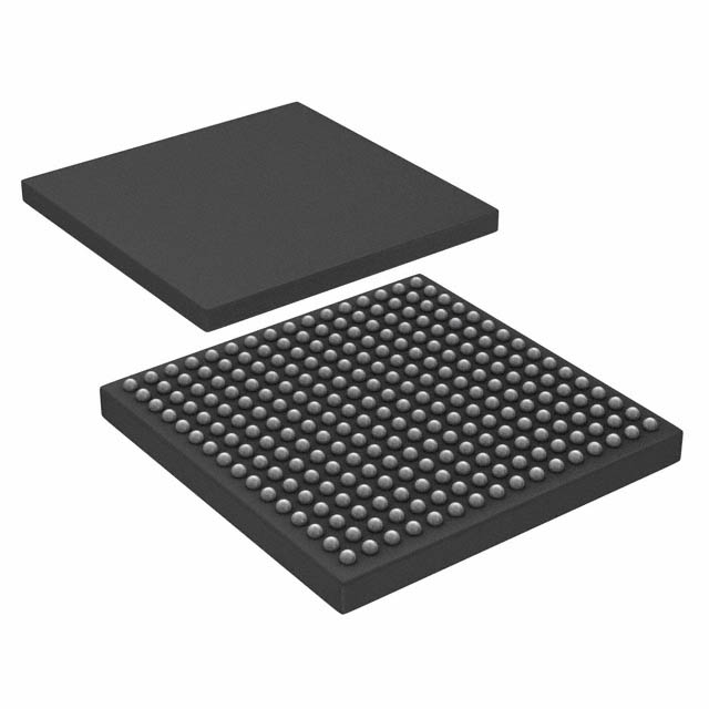
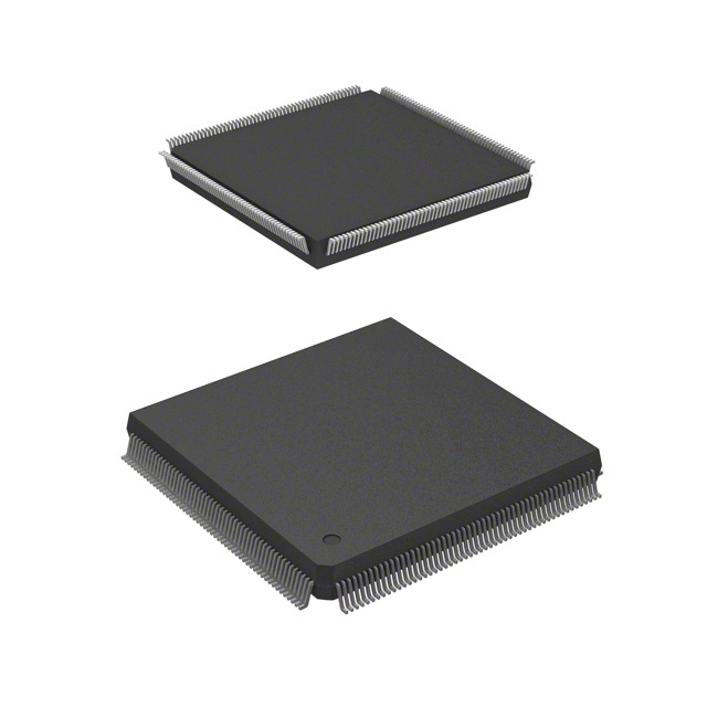
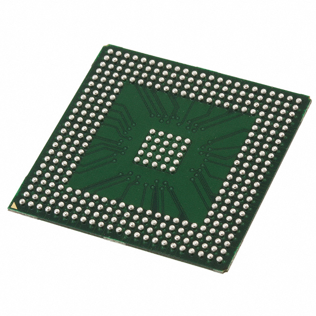
SX-A Field Programmable Gate Array (FPGA) IC 249 329-BBGA |
|---|---|
| Quantity | 370 Available (as of June 14, 2026) |

| Product Category | Field Programmable Gate Array (FPGA) |
|---|---|
| Manufacturer | Microchip Technology |
| Manufacturing Status | Active |
| Manufacturer Standard Lead Time | 20 Weeks |
| Datasheet |
Specifications & Environmental
| Device Package | 329-PBGA (31x31) | Grade | Military | Operating Temperature | -55°C – 125°C | ||
|---|---|---|---|---|---|---|---|
| Package / Case | 329-BBGA | Number of I/O | 249 | Voltage | 2.25 V - 5.25 V | ||
| Mounting Method | Surface Mount | RoHS Compliance | ROHS3 Compliant | REACH Compliance | REACH Unaffected | ||
| Moisture Sensitivity Level | 3 (168 Hours) | Number of LABs/CLBs | 2880 | Number of Logic Elements/Cells | 2880 | ||
| Number of Gates | 48000 | ECCN | 3A001A2C | HTS Code | 8542.39.0001 | ||
| Qualification | N/A |
Overview of A54SX32A-1BGG329M – SX-A Field Programmable Gate Array (FPGA) IC 249 329-BBGA
The A54SX32A-1BGG329M is a military-grade SX-A family FPGA provided in a 329-ball BGA package. It combines nonvolatile single-chip FPGA architecture with high I/O density and a wide operating temperature range for rugged, mission-critical designs.
Designed for applications that require secure, high-density logic and flexible interfacing, this device offers 48,000 system gates and 2,880 logic elements with a 249-pin I/O count, supporting mixed-voltage operation and supplier-standard BGA packaging.
Key Features
- Logic Capacity — 48,000 system gates and approximately 2,880 logic elements for implementing complex logic functions and state machines.
- User I/O and Voltage Flexibility — 249 user I/Os with family-level support for configurable I/O standards and mixed-voltage operation; device supply range 2.25 V to 5.25 V for flexible board-level integration.
- Nonvolatile Single-Chip Architecture — SX-A family nonvolatile configuration eliminates the need for external configuration memory and supports reliable power-up behavior.
- Performance (SX-A Family) — SX-A family data indicates system performance up to 250 MHz and internal performance up to 350 MHz for timing-sensitive designs.
- Security and Test — Family features include Actel Secure Programming Technology (FuseLock™) to protect design IP and IEEE 1149.1 (JTAG) boundary-scan support for board-level testability.
- Rugged Packaging and Mounting — Supplied in a 329-PBGA (31 × 31 mm) surface-mount package (329-BBGA case) suitable for compact, high-density PCB layouts.
- Wide Temperature Range — Military-grade operating temperature from −55 °C to +125 °C for deployment in harsh environments.
- Regulatory — RoHS compliant.
- On-chip Memory — No embedded RAM bits; design flows should account for off-chip memory if required.
Typical Applications
- Military and Aerospace Systems — Military temperature grade and nonvolatile configuration make the device suitable for rugged avionics, tactical electronics, and other defense applications.
- Secure Embedded Logic — Built-in programming security (FuseLock™) and single-chip configuration support secure implementations where IP protection and controlled provisioning matter.
- High-Density Interface Bridging — 249 user I/Os and mixed-voltage support allow consolidation of multiple interfaces and protocol bridging on a single FPGA.
- Deterministic Control and Timing — Family-level performance characteristics and deterministic timing features are well suited for embedded control, instrumentation, and timing-sensitive subsystems.
Unique Advantages
- Military-Grade Reliability: Qualified for −55 °C to +125 °C operation, supporting deployments in extreme environments.
- High I/O Count: 249 user I/Os enable complex system integration and reduce the need for additional interface components.
- Nonvolatile, Single-Chip Solution: Eliminates external configuration memory, simplifying power sequencing and improving system robustness.
- Flexible Supply Range: 2.25 V to 5.25 V supply range provides design flexibility across different board-level voltage architectures.
- Design Security and Testability: FuseLock™ secure programming and IEEE 1149.1 JTAG support protect IP and facilitate boundary-scan testing.
- Compact BGA Packaging: 329-ball PBGA (31 × 31 mm) package delivers high pin count in a compact footprint for space-constrained systems.
Why Choose A54SX32A-1BGG329M?
The A54SX32A-1BGG329M targets designs that require a robust, nonvolatile FPGA with high I/O density and military-grade temperature performance. With 48,000 system gates, approximately 2,880 logic elements, and 249 user I/Os, it supports complex logic integration and interface consolidation while operating across a wide supply range (2.25 V–5.25 V).
Its single-chip nonvolatile architecture, programmable security features, and RoHS compliance deliver long-term reliability and IP protection for demanding applications where environmental tolerance and secure provisioning are priorities.
Request a quote or submit an inquiry to our sales team for pricing, availability, and lead-time information on the A54SX32A-1BGG329M.


Date Founded: 1989
Headquarters: Chandler, Arizona, USA
Employees: 22,000+
Revenue: $8.349 Billion
Certifications and Memberships: ISO9001:2015, IATF16949:2016, AS 9100D


