
A54SX32A-1CQ208B
| Part Description |
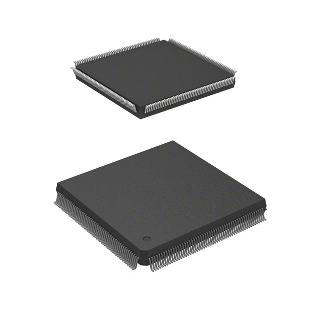
SX-A Field Programmable Gate Array (FPGA) IC 174 208-BFCQFP with Tie Bar |
|---|---|
| Quantity | 763 Available (as of June 15, 2026) |
| Product Category | Field Programmable Gate Array (FPGA) |
|---|---|
| Manufacturer | Microchip Technology |
| Manufacturing Status | Active |
| Manufacturer Standard Lead Time | 40 Weeks |
| Datasheet |
Specifications & Environmental
| Device Package | 208-CQFP (75x75) | Grade | Military | Operating Temperature | -55°C – 125°C | ||
|---|---|---|---|---|---|---|---|
| Package / Case | 208-BFCQFP with Tie Bar | Number of I/O | 174 | Voltage | 2.25 V - 5.25 V | ||
| Mounting Method | Surface Mount | RoHS Compliance | RoHS non-compliant | REACH Compliance | REACH Unaffected | ||
| Moisture Sensitivity Level | 3 (168 Hours) | Number of LABs/CLBs | 2880 | Number of Logic Elements/Cells | 2880 | ||
| Number of Gates | 48000 | ECCN | 3A001A2C | HTS Code | 8542.39.0001 | ||
| Qualification | N/A |
Overview of A54SX32A-1CQ208B – SX-A Field Programmable Gate Array (FPGA) – 174 I/O, 208‑BFCQFP
The A54SX32A-1CQ208B is a military‑grade SX‑A family FPGA from Microchip Technology, offered in a 208‑pin ceramic CQFP package with tie bar. It delivers a deterministic, high‑reliability FPGA architecture tailored for systems requiring rugged temperature performance and secure configuration options.
With 2,880 logic elements (approximately 48,000 system gates) and 174 user I/Os in the 208‑pin package, this device is suited to high‑reliability embedded and defense applications that demand broad voltage support, stringent temperature qualification, and robust configuration security.
Key Features
- Logic Capacity – 2,880 logic elements (listed) providing approximately 48,000 system gates for combinational and sequential logic implementation.
- I/O and Pin Count – 174 user‑programmable I/Os in the 208‑pin CQFP package to support complex interfacing and multi‑voltage systems.
- Voltage Supply – Supports a supply range of 2.25 V to 5.25 V, enabling flexible power architectures and mixed‑voltage designs.
- Temperature and Grade – Military grade device with an operating temperature range of −55 °C to +125 °C and Class B (MIL‑STD‑883) flow options as documented for the SX‑A family.
- Package and Mounting – Supplied in a 208‑BFCQFP ceramic package with tie bar; surface‑mount mounting type. Supplier device package listed as 208‑CQFP (75×75).
- High‑Reliability Family Features – Family datasheet documents QML certification, 100% military‑temperature testing, boundary‑scan (IEEE 1149.1 JTAG), and secure programming technology (FuseLock™) for protection against reverse engineering.
- Performance Indicators (Family) – Family datasheet reports up to 215 MHz system performance and 5.3 ns clock‑to‑out at military temperatures for SX‑A devices; consult device datasheet tables for specific timing values.
- RoHS Compliance – Device is RoHS compliant as listed in the product data.
Typical Applications
- Military and Aerospace Systems – Suitable for mission‑critical control, signal processing, and data‑handling functions where military temperature range and QML flow are required.
- Avionics and Embedded Control – Use for control logic, interface bridging, and deterministic timing functions that benefit from the SX‑A family’s timing characteristics and boundary‑scan support.
- Communications and Radar Subsystems – Interfaces and processing blocks that require numerous I/Os and reliable operation across a wide temperature range.
- High‑Reliability Instrumentation – Lab and field instrumentation that needs ceramic packaging, secure programming, and burn‑in/test regimes consistent with MIL‑STD‑883 flow.
Unique Advantages
- Military‑grade qualification: The device is specified for −55 °C to +125 °C operation and is offered in Class B/MIL flows documented for the SX‑A family, supporting high‑reliability deployments.
- Secure configuration: Family documentation lists Actel Secure Programming Technology (FuseLock™) to protect bitstream confidentiality and intellectual property.
- Broad I/O and voltage flexibility: 174 user I/Os in the 208‑pin package and a wide supply range (2.25 V–5.25 V) enable mixed‑voltage interfacing and flexible board designs.
- Deterministic timing and testability: SX‑A family timing characteristics and IEEE 1149.1 boundary‑scan support simplify deterministic design and manufacturing test strategies.
- Ceramic CQFP packaging: 208‑pin ceramic CQFP with tie bar provides package robustness and is compatible with surface‑mount assembly for rugged systems.
Why Choose A54SX32A-1CQ208B?
The A54SX32A-1CQ208B combines a mid‑density logic resource set (2,880 logic elements / ~48,000 system gates) with a broad I/O complement and proven HiRel SX‑A family attributes such as secure programming, boundary‑scan, and documented military qualification flows. Its wide supply range and ceramic 208‑pin CQFP packaging make it a practical choice for designers targeting military, aerospace, and other high‑reliability embedded applications.
This part is ideal for teams needing deterministic FPGA resources with secure configuration and rigorous temperature qualification. The device’s combination of logic capacity, I/O availability, and family‑level testing and security features supports long‑lifecycle programs where robustness and traceable qualification are important.
Request a quote or submit an RFQ for A54SX32A-1CQ208B to begin procurement or to discuss availability and ordering options.


Date Founded: 1989
Headquarters: Chandler, Arizona, USA
Employees: 22,000+
Revenue: $8.349 Billion
Certifications and Memberships: ISO9001:2015, IATF16949:2016, AS 9100D


