
A54SX32A-1CQ256B
| Part Description |
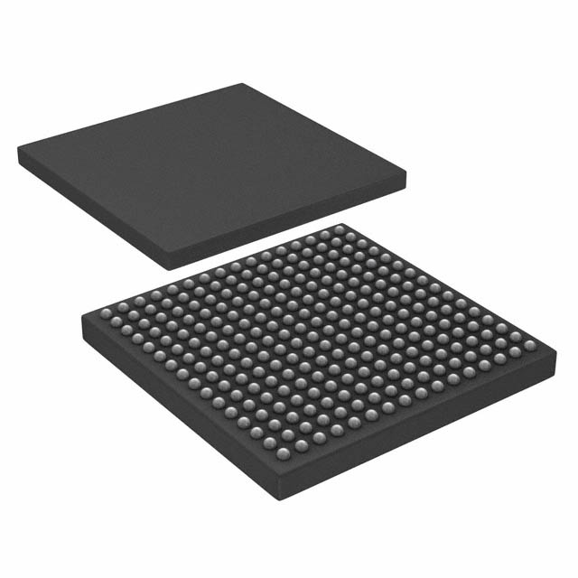
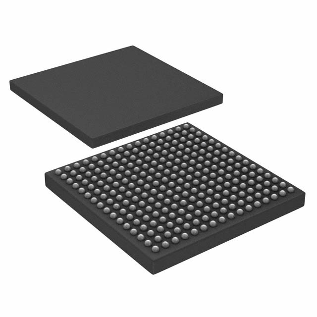
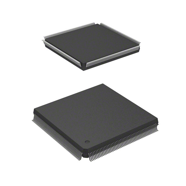
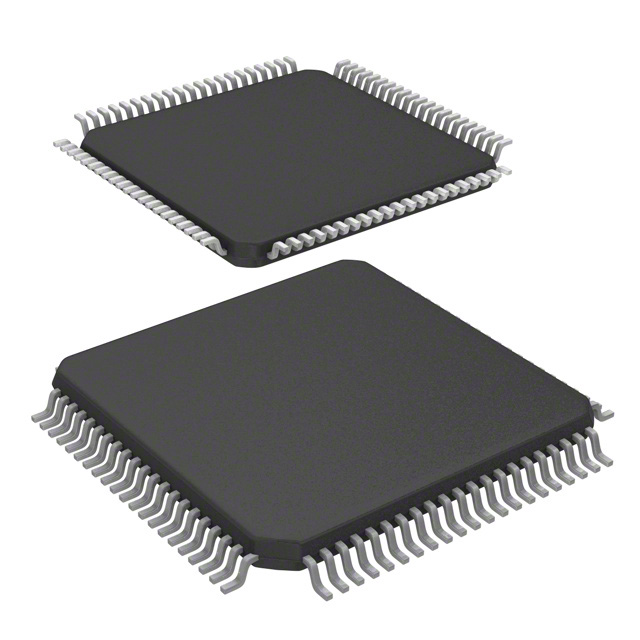
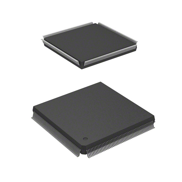
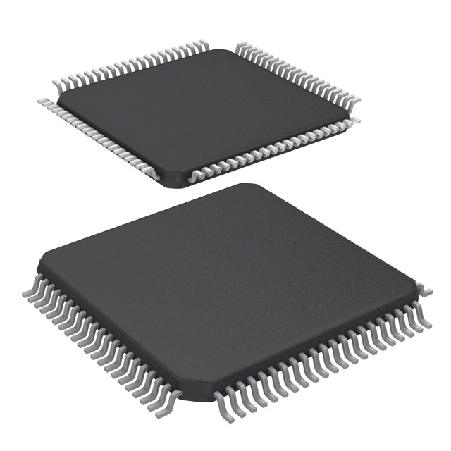
SX-A Field Programmable Gate Array (FPGA) IC 203 256-BFCQFP with Tie Bar |
|---|---|
| Quantity | 1,427 Available (as of October 8, 2026) |
| Product Category | Field Programmable Gate Array (FPGA) |
|---|---|
| Manufacturer | Microchip Technology |
| Manufacturing Status | Active |
| Manufacturer Standard Lead Time | 44 Weeks |
| Datasheet |
Specifications & Environmental
| Device Package | 256-CQFP (75x75) | Grade | Military | Operating Temperature | -55°C – 125°C | ||
|---|---|---|---|---|---|---|---|
| Package / Case | 256-BFCQFP with Tie Bar | Number of I/O | 203 | Voltage | 2.25 V - 5.25 V | ||
| Mounting Method | Surface Mount | RoHS Compliance | RoHS non-compliant | REACH Compliance | REACH Unaffected | ||
| Moisture Sensitivity Level | 3 (168 Hours) | Number of LABs/CLBs | 2880 | Number of Logic Elements/Cells | 2880 | ||
| Number of Gates | 48000 | ECCN | 3A001A2C | HTS Code | 8542.39.0001 | ||
| Qualification | N/A |
Overview of A54SX32A-1CQ256B – SX-A Field Programmable Gate Array (FPGA) IC 203 256-BFCQFP with Tie Bar
The A54SX32A-1CQ256B is a military-grade FPGA from the HiRel SX-A family by Microchip Technology, delivered in a 256‑lead ceramic CQFP package with tie bar for surface-mount assembly. It provides a deterministic, secure programmable logic solution optimized for mission-critical and high-reliability embedded designs.
Built around 48,000 system gates and approximately 2,880 logic elements, this device targets applications that require high-speed system performance, robust I/O flexibility and proven military temperature qualification.
Key Features
- Core Performance 48,000 system gates and 2,880 logic elements provide deterministic logic capacity. Specified family performance includes up to 215 MHz system performance and 5.3 ns clock‑to‑out at military temperature.
- Logic & Flip‑Flop Resources Dedicated flip‑flop resources referenced in the SX‑A family enable consistent, user‑controllable timing for synchronous designs.
- I/O and Interface Flexibility 203 user I/O pins (surface mount) with hot‑swap compliant I/Os and configurable I/O support for 3.3 V / 5 V PCI, LVTTL and TTL signaling modes as defined by the SX‑A family.
- Voltage and Power Wide supply range from 2.25 V to 5.25 V and power‑up/power‑down friendly operation (no sequencing required for supply voltages), enabling mixed‑voltage system integration.
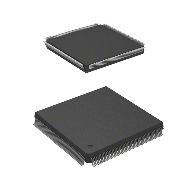
- Package and Mounting 256‑BFCQFP with tie bar (supplier device package: 256‑CQFP, 75 × 75) in a surface‑mount form factor suitable for high‑reliability assemblies.
- Military Qualification & Temperature Range Military grade device with operating range −55 °C to +125 °C and family-level QML and MIL‑STD‑883 process flow and testing described in the datasheet.
- Security & Testability Actel Secure Programming Technology with FuseLock to protect against reverse engineering and design theft; boundary‑scan (IEEE 1149.1 JTAG) support for in‑system test and debug.
- Memory Device listing shows zero on‑chip RAM bits, focusing the device on dedicated logic and flip‑flop implementations.
Typical Applications
- Military & Aerospace Systems Deployed where MIL temperature performance and QML/MIL‑STD‑883 testing support are required for mission‑critical logic functions.
- PCI‑Based Subsystems Suitable for implementing PCI interface logic and bridge functions with 3.3 V / 5 V PCI support and 5 V input tolerance documented at the family level.
- Secure, Embedded Control Used for secure programmable logic blocks where FuseLock programming and deterministic timing are important for protecting IP and ensuring predictable behavior.
- High‑Reliability Instrumentation Ideal for control, timing, and glue‑logic in instrumentation that requires ceramic packaging, wide supply range and extended temperature operation.
Unique Advantages
- Military‑grade qualification: The device is specified for −55 °C to +125 °C operation and follows MIL‑STD‑883 product flow and testing, supporting high‑reliability deployments.
- Deterministic timing: Family-level timing metrics such as 5.3 ns clock‑to‑out and predictable internal timing simplify timing closure for synchronous designs.
- Secure programming: FuseLock secure programming capability helps protect design IP from reverse engineering and unauthorized access.
- Flexible I/O and voltage tolerance: Wide supply range (2.25 V–5.25 V) and configurable I/O modes support mixed‑voltage system integration and PCI signaling needs.
- Proven ceramic packaging: 256‑lead ceramic CQFP with tie bar offers a rugged form factor suited to harsh environment assemblies and board‑level reliability.
- Power sequencing immunity: Power‑up/power‑down friendly operation reduces constraints during system power transitions and simplifies board power design.
Why Choose A54SX32A-1CQ256B?
The A54SX32A-1CQ256B positions itself as a deterministic, secure FPGA option for designers who need military‑grade performance and ceramic packaging. With 48,000 system gates, 2,880 logic elements, 203 user I/Os, and family-proven timing and security features, it is suited to embedded systems where reliability, predictable timing and IP protection are priorities.
Choose this device when your project demands proven MIL testing, flexible voltage/I/O support and a ceramic surface‑mount package for long‑life, high‑reliability deployments.
Request a quote to check availability, lead times and pricing for the A54SX32A-1CQ256B. Submit your requirements to initiate procurement or evaluate this device for your next high‑reliability FPGA design.





















Date Founded: 1989
Headquarters: Chandler, Arizona, USA
Employees: 22,000+
Revenue: $8.349 Billion
Certifications and Memberships: ISO9001:2015, IATF16949:2016, AS 9100D




