
A54SX32A-1CQ84B
| Part Description |
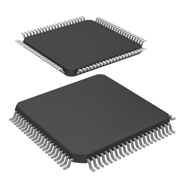
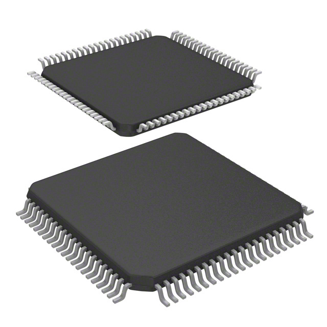
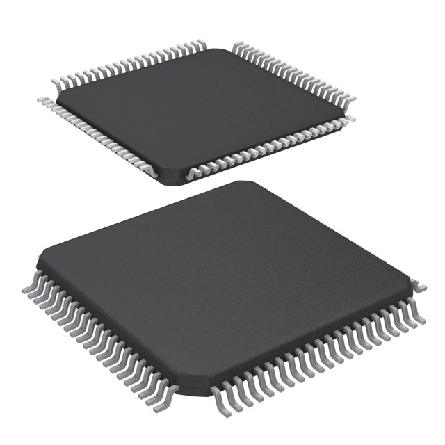
SX-A Field Programmable Gate Array (FPGA) IC 69 84-CQFP Exposed Pad and Tie Bar |
|---|---|
| Quantity | 1,735 Available (as of October 8, 2026) |
| Product Category | Field Programmable Gate Array (FPGA) |
|---|---|
| Manufacturer | Microchip Technology |
| Manufacturing Status | Active |
| Manufacturer Standard Lead Time | 44 Weeks |
| Datasheet |
Specifications & Environmental
| Device Package | 84-CQFP (42x42) | Grade | Military | Operating Temperature | -55°C – 125°C | ||
|---|---|---|---|---|---|---|---|
| Package / Case | 84-CQFP Exposed Pad and Tie Bar | Number of I/O | 69 | Voltage | 2.25 V - 5.25 V | ||
| Mounting Method | Surface Mount | RoHS Compliance | RoHS non-compliant | REACH Compliance | REACH Unaffected | ||
| Moisture Sensitivity Level | 3 (168 Hours) | Number of LABs/CLBs | 2880 | Number of Logic Elements/Cells | 2880 | ||
| Number of Gates | 48000 | ECCN | 3A001A2C | HTS Code | 8542.39.0001 | ||
| Qualification | N/A |
Overview of A54SX32A-1CQ84B – SX-A Field Programmable Gate Array, 69 I/O, 84-CQFP
The A54SX32A-1CQ84B is a military-grade SX-A family FPGA from Microchip Technology, delivered in an 84-pin ceramic CQFP package with exposed pad and tie bar. It combines deterministic FPGA architecture with high-reliability manufacturing and military temperature qualification for demanding embedded systems.
Designed for applications that require robust operation across extremes, this device provides 48,000 system gates and 2,880 logic elements with up to 69 user I/Os and mixed-voltage operation across a wide supply range.
Key Features
- Core Capacity 48,000 system gates and approximately 2,880 logic elements provide programmable logic density suitable for complex control and glue-logic tasks.
- I/O and Packaging 69 user I/Os in an 84-pin CQFP (42 × 42 mm) ceramic package with exposed pad and tie bar; surface-mount package designed for high-reliability assemblies.
- Operating Range Military-grade operation from −55 °C to +125 °C, with Class B device screening and MIL-STD-883 product flow noted for the family.
- Voltage Flexibility Wide supply range from 2.25 V to 5.25 V supporting mixed-voltage designs and legacy interface requirements.
- Series Performance Characteristics Series-level performance indications include up to 215 MHz system performance and 5.3 ns clock-to-out at military temperature conditions (series specification).
- No Embedded RAM Total on-chip RAM bits: 0 — suitable where deterministic logic resources are the primary requirement.
- Reliability and Compliance Military-grade screening, QML/Class B level device characteristics and RoHS compliance for environmental requirements.
- Advanced Series Features The SX-A family provides secure programming technology (FuseLock), boundary-scan (JTAG) capabilities, and hot-swap–capable I/Os as part of the series feature set.
Typical Applications
- Military and Aerospace Systems Rugged temperature range and military-grade qualification make this FPGA suitable for avionics, tactical electronics, and other harsh-environment subsystems.
- High-Reliability Embedded Control Use as a single-chip configurable logic solution for reliability-focused control, signal conditioning, and interface bridging where predictable timing is required.
- Legacy and Mixed-Voltage Interfaces Wide supply range and series support for mixed 2.5 V/3.3 V/5 V operation allow integration with legacy TTL/LVTTL and PCI-style interfaces.
Unique Advantages
- Military-Grade Screening: Delivered with military temperature testing and Class B device flow for projects that require thorough environmental qualification.
- Deterministic Timing: Series-level clock-to-output and internal performance metrics support designs that need predictable, low-latency logic paths.
- Flexible I/O Packaging: 69 user I/Os in a compact 84-CQFP ceramic package with exposed pad supports dense board layouts while maintaining thermal and mechanical robustness.
- Wide Supply Compatibility: 2.25 V to 5.25 V operation accommodates mixed-voltage systems and simplifies integration with a variety of peripherals.
- Security and Testability: Series features include secure programming (FuseLock) and boundary-scan (JTAG) for IP protection and manufacturing testability.
- No On-Chip RAM (Deterministic Logic): With zero on-chip RAM bits, the device is focused on predictable logic resources for timing-critical applications.
Why Choose A54SX32A-1CQ84B?
The A54SX32A-1CQ84B positions itself as a high-reliability FPGA option within the SX-A family for engineers building systems that demand military temperature performance, deterministic timing, and secure programmable logic. Its 48,000 system gates and 2,880 logic elements provide substantial programmable capacity while the 69 I/Os and flexible supply range ease integration across mixed-voltage environments.
This device is well-suited to customers designing aerospace, defense, and other mission-critical embedded systems where long-term robustness, qualification, and series-level security/test features are primary considerations.
Request a quote or contact sales to submit an RFQ for the A54SX32A-1CQ84B and evaluate its fit for your high-reliability design needs.





















Date Founded: 1989
Headquarters: Chandler, Arizona, USA
Employees: 22,000+
Revenue: $8.349 Billion
Certifications and Memberships: ISO9001:2015, IATF16949:2016, AS 9100D




