
A54SX32A-1FG256I
| Part Description |
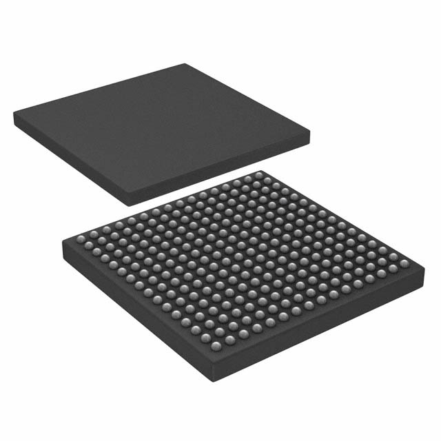
SX-A Field Programmable Gate Array (FPGA) IC 203 256-BGA |
|---|---|
| Quantity | 670 Available (as of June 18, 2026) |
| Product Category | Field Programmable Gate Array (FPGA) |
|---|---|
| Manufacturer | Microchip Technology |
| Manufacturing Status | Active |
| Manufacturer Standard Lead Time | 12 Weeks |
| Datasheet |
Specifications & Environmental
| Device Package | 256-FPBGA (17x17) | Grade | Industrial | Operating Temperature | -40°C – 85°C | ||
|---|---|---|---|---|---|---|---|
| Package / Case | 256-BGA | Number of I/O | 203 | Voltage | 2.25 V - 5.25 V | ||
| Mounting Method | Surface Mount | RoHS Compliance | RoHS non-compliant | REACH Compliance | REACH Unaffected | ||
| Moisture Sensitivity Level | 3 (168 Hours) | Number of LABs/CLBs | 2880 | Number of Logic Elements/Cells | 2880 | ||
| Number of Gates | 48000 | ECCN | 3A991D | HTS Code | 8542.39.0001 | ||
| Qualification | N/A |
Overview of A54SX32A-1FG256I – SX-A Field Programmable Gate Array (FPGA) IC 203 256-BGA
The A54SX32A-1FG256I is a nonvolatile SX-A family FPGA in a 256-ball fine-pitch BGA package designed for industrial applications. It provides a programmable logic platform with approximately 48,000 system gates and 2,880 logic elements, supporting up to 203 user I/Os for complex interface and control tasks.
Built for mixed-voltage systems and in-system verification, this device targets industrial control, interface bridging and embedded logic functions where deterministic timing, configurability and on-board security are required.
Key Features
- Logic Capacity — Approximately 48,000 system gates and 2,880 logic elements to implement medium-density digital designs.
- User I/O — Up to 203 user-programmable I/Os, configurable for multiple signaling standards and with individual slew-rate control.
- Performance — SX-A family performance characteristics including up to 250 MHz system performance and up to 350 MHz internal performance (series specification).
- Nonvolatile Single-Chip Solution — On-chip nonvolatile configuration for single-chip system architectures and instant-on behavior.
- Voltage Flexibility — Operates across a wide supply range (2.25 V to 5.25 V) enabling mixed-voltage interfacing and 5 V input tolerance where supported.
- Industrial Temperature Grade — Rated for operation from −40 °C to +85 °C, suitable for industrial environments.
- Package and Mounting — 256-ball fine-pitch BGA (256-FPBGA, 17×17) surface-mount package for dense board-level integration.
- Security and Test — Includes Actel Secure Programming Technology with FuseLock™ for intellectual-property protection and IEEE 1149.1 (JTAG) boundary-scan testing support.
- System-Friendly I/Os — Hot-swap compliant I/Os and power-up/power-down friendly behavior (no sequencing required for supply voltages).
- Regulatory — RoHS compliant.
Typical Applications
- Industrial Control and Automation — Leverages industrial temperature rating and flexible I/O for control logic, protocol bridging and deterministic interface functions.
- PCI Interface Logic — Supports 66 MHz PCI-compliant signaling and configurable I/O levels for PCI-related glue logic and bridge functions.
- In-System Verification and Test — Boundary-scan (IEEE 1149.1) and in-system diagnostic capabilities facilitate board-level validation and production test workflows.
- Secure Embedded Logic — Nonvolatile configuration with FuseLock™ protection for designs requiring IP security and controlled field programmability.
Unique Advantages
- Deterministic, Controllable Timing: SX-A family timing characteristics support predictable timing behavior for time-critical designs.
- Wide Supply Range: 2.25 V to 5.25 V operation allows direct interfacing with legacy 5 V systems and modern lower-voltage domains.
- Industrial Qualification: −40 °C to +85 °C temperature range and surface-mount 256-FPBGA package suited to industrial deployment.
- Integrated Security: Actel FuseLock™ technology adds protection against reverse engineering and unauthorized copying of design bitstreams.
- Production and Diagnostics: JTAG boundary-scan and in-system diagnostic features streamline manufacturing test and field verification.
- High I/O Count in Compact Package: 203 user I/Os in a 17×17 256-FPBGA provide dense connectivity for multi-interface applications.
Why Choose A54SX32A-1FG256I?
The A54SX32A-1FG256I offers a balanced combination of medium-density logic capacity, flexible I/O and production-oriented features in a single nonvolatile FPGA package. Its mix of industry-grade temperature range, wide supply tolerance and security features makes it well suited to embedded system designs that require reliable operation, field configurability and IP protection.
This device is appropriate for engineering teams and procurement groups seeking a programmable, single-chip solution for industrial control, interface bridging, and secure embedded logic with on-board diagnostic and boundary-scan support.
Request a quote or submit a sales inquiry to learn about availability, lead times and volume pricing for the A54SX32A-1FG256I.


Date Founded: 1989
Headquarters: Chandler, Arizona, USA
Employees: 22,000+
Revenue: $8.349 Billion
Certifications and Memberships: ISO9001:2015, IATF16949:2016, AS 9100D


