
A54SX32A-1FGG256
| Part Description |
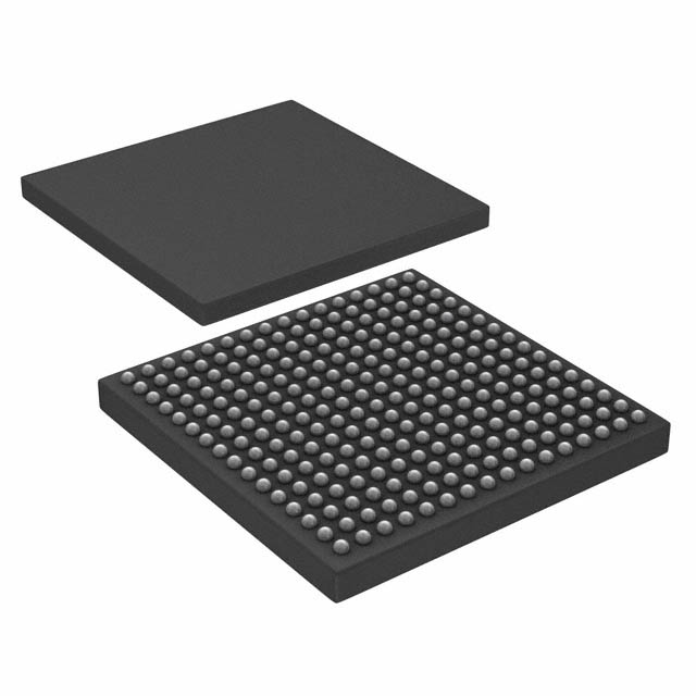
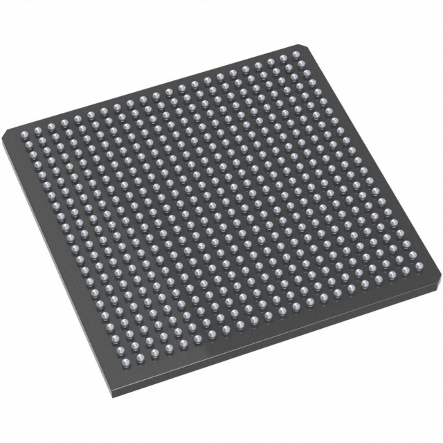
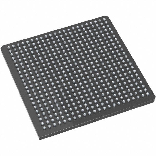
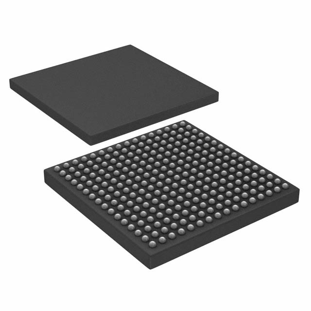
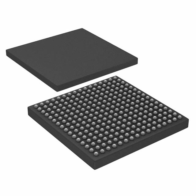
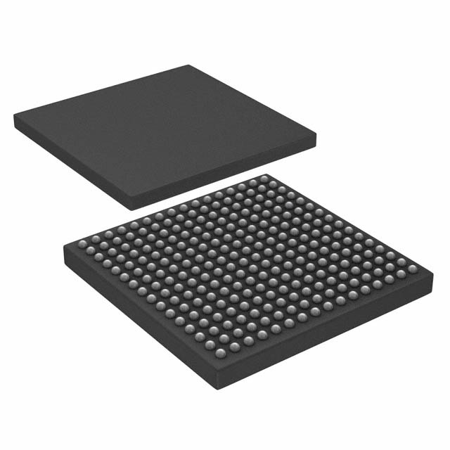
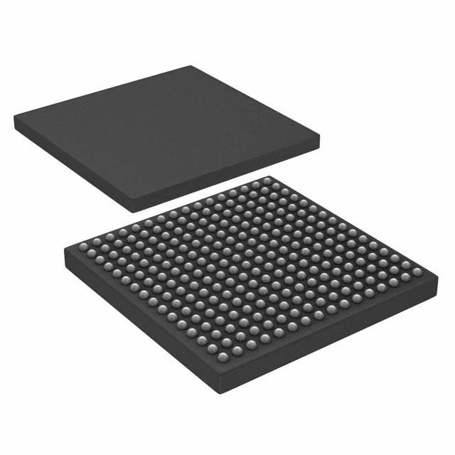
SX-A Field Programmable Gate Array (FPGA) IC 203 256-BGA |
|---|---|
| Quantity | 201 Available (as of October 8, 2026) |

| Product Category | Field Programmable Gate Array (FPGA) |
|---|---|
| Manufacturer | Microchip Technology |
| Manufacturing Status | Active |
| Manufacturer Standard Lead Time | 12 Weeks |
| Datasheet |
Specifications & Environmental
| Device Package | 256-FPBGA (17x17) | Grade | Commercial | Operating Temperature | 0°C – 70°C | ||
|---|---|---|---|---|---|---|---|
| Package / Case | 256-BGA | Number of I/O | 203 | Voltage | 2.25 V - 5.25 V | ||
| Mounting Method | Surface Mount | RoHS Compliance | ROHS3 Compliant | REACH Compliance | REACH Unaffected | ||
| Moisture Sensitivity Level | 3 (168 Hours) | Number of LABs/CLBs | 2880 | Number of Logic Elements/Cells | 2880 | ||
| Number of Gates | 48000 | ECCN | 3A991D | HTS Code | 8542.39.0001 | ||
| Qualification | N/A |
Overview of A54SX32A-1FGG256 – SX-A Field Programmable Gate Array (FPGA) IC 203 256-BGA
The A54SX32A-1FGG256 is a Commercial-grade SX‑A family FPGA from Microchip Technology provided as a nonvolatile, single‑chip programmable logic device. It delivers 48,000 system gates across approximately 2,880 logic elements and provides 203 user I/Os in a 256‑ball fine‑pitch BGA package.
Designed for applications that require reprogrammable logic with wide I/O flexibility and mixed‑voltage support, the device supports a broad supply range and in-system programmability while meeting RoHS requirements.
Key Features
- Logic Capacity — Approximately 48,000 system gates implemented across about 2,880 logic elements, enabling medium‑complexity combinatorial and sequential logic integration.
- User I/O — 203 configurable user I/Os to support dense external connectivity and peripheral interfacing.
- Nonvolatile Single‑Chip Solution — In‑system programmable, single‑chip FPGA architecture that eliminates the need for external configuration memory.
- Performance — SX‑A family performance characteristics include published system and internal frequency points (family level: up to 250 MHz system performance and up to 350 MHz internal performance).
- Mixed‑Voltage I/O and Supply Range — Configurable I/O support for multiple voltage standards (family level), with a device supply range of 2.25 V to 5.25 V enabling mixed‑voltage system designs.
- Package and Mounting — 256‑ball fine‑pitch BGA (256‑FPBGA, 17×17) in a surface‑mount package; FG (fine pitch) package option with 1.0 mm ball pitch.
- Commercial Temperature Grade — Rated for commercial operation from 0 °C to 70 °C.
- Security and Test — Family features include Secure Programming technology (FuseLock™) and boundary‑scan (IEEE 1149.1) support for design protection and manufacturing testability.
- Regulatory — RoHS compliant.
- Speed Grade — This part is the –1 speed grade (family guidance indicates –1 is approximately 15% faster than standard).
Typical Applications
- PCI and bus interface logic — Family support for 66 MHz PCI and configurable I/O standards makes the device suitable for implementing PCI interface logic and bus bridges.
- Custom glue logic and I/O expansion — Use the device to consolidate discrete glue logic and implement complex I/O interfacing with its 203 user I/Os.
- In‑system programmable control — Ideal for designs that benefit from field reprogrammability and in‑system verification capabilities provided by SX‑A family tooling.
Unique Advantages
- High I/O density: 203 user‑programmable I/Os enable broad external connectivity without additional interface chips.
- Nonvolatile, single‑chip configuration: On‑chip configuration removes the need for external configuration memory, simplifying system BOM and board layout.
- Flexible supply and I/O voltages: 2.25 V to 5.25 V device supply supports mixed‑voltage designs and multiple I/O standards at the family level.
- Security and testability: On‑device security (FuseLock™) and IEEE 1149.1 boundary‑scan support protect intellectual property and streamline manufacturing test.
- Commercial grade reliability: Rated for 0 °C to 70 °C operation and RoHS compliance for standard commercial deployments.
- Deterministic timing control: Family features include user‑controllable timing characteristics for predictable system behavior.
Why Choose A54SX32A-1FGG256?
The A54SX32A-1FGG256 packages a medium‑capacity, nonvolatile FPGA into a compact 256‑ball fine‑pitch BGA with 203 I/Os and approximately 48,000 system gates. Its family‑level performance characteristics, mixed‑voltage I/O support, and built‑in security and test features make it a practical choice for designers needing reprogrammable logic, robust I/O connectivity, and in‑system programmability within a commercial temperature envelope.
This device is well suited to teams and projects that require an integrated programmable logic solution to reduce board complexity and streamline system integration while retaining field reprogrammability and manufacturing test support.
Request a quote or submit a pricing inquiry for the A54SX32A-1FGG256 to receive availability and purchasing information.





















Date Founded: 1989
Headquarters: Chandler, Arizona, USA
Employees: 22,000+
Revenue: $8.349 Billion
Certifications and Memberships: ISO9001:2015, IATF16949:2016, AS 9100D




