
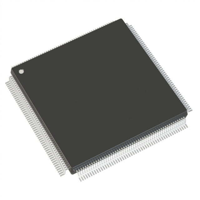
A54SX32A-1PQ208
| Part Description |
SX-A Field Programmable Gate Array (FPGA) IC 174 208-BFQFP |
|---|---|
| Quantity | 979 Available (as of June 15, 2026) |
| Product Category | Field Programmable Gate Array (FPGA) |
|---|---|
| Manufacturer | Microchip Technology |
| Manufacturing Status | Obsolete |
| Manufacturer Standard Lead Time | Contact Us |
| Datasheet |
Specifications & Environmental
| Device Package | 208-PQFP (28x28) | Grade | Commercial | Operating Temperature | 0°C – 70°C | ||
|---|---|---|---|---|---|---|---|
| Package / Case | 208-BFQFP | Number of I/O | 174 | Voltage | 2.25 V - 5.25 V | ||
| Mounting Method | Surface Mount | RoHS Compliance | RoHS non-compliant | REACH Compliance | REACH Unaffected | ||
| Moisture Sensitivity Level | 3 (168 Hours) | Number of LABs/CLBs | 2880 | Number of Logic Elements/Cells | 2880 | ||
| Number of Gates | 48000 | ECCN | 3A991D | HTS Code | 8542.39.0001 | ||
| Qualification | N/A |
Overview of A54SX32A-1PQ208 – SX-A Field Programmable Gate Array (FPGA) IC 174 208-BFQFP
The A54SX32A-1PQ208 is a member of the SX-A family of nonvolatile, single-chip FPGAs. It provides a mid-range programmable logic fabric with 2,880 logic elements and 48,000 system gates in a 208-pin BFQFP/PQFP footprint, targeting commercial-temperature embedded and interface designs.
Designed for applications requiring configurable I/O flexibility and deterministic timing, the device supports mixed-voltage I/O, hot-swap–capable signals and in-system diagnostics while operating from a 2.25 V to 5.25 V supply and a commercial temperature range of 0 °C to 70 °C.
Key Features
- Logic Capacity — 2,880 logic elements (combinatorial cells) delivering approximately 48,000 system gates and up to 2,012 dedicated flip-flops for implementing mid-density programmable logic.
- User I/O — 174 user-programmable I/O pins in the 208-pin package with configurable I/O support for multiple signaling levels and 5 V input tolerance as described in the SX-A family documentation.
- Performance — SX-A family performance characteristics include up to 250 MHz system performance and up to 350 MHz internal performance; this specific device is offered in the –1 speed grade (approximately 15% faster than standard).
- Power and Voltage Flexibility — Single-device operation across a 2.25 V to 5.25 V supply range and support for mixed-voltage (2.5 V, 3.3 V and 5 V) operation for flexible interfacing.
- Packaging and Mounting — Surface-mount 208-pin BFQFP (supplier package: 208-PQFP, 28×28) suitable for compact board-level integration in commercial designs.
- System and Diagnostic Features — Nonvolatile, single-chip configuration (no external configuration memory required), boundary-scan testing compliant with IEEE 1149.1 (JTAG), and in-system diagnostic/verification capability as provided by the SX-A family.
- I/O Reliability — Hot-swap–compliant I/Os and configurable weak pull-up or pull-down options at power-up to support robust board-level behavior.
- Regulatory Status — RoHS compliant.
- Operating Grade — Commercial temperature grade (0 °C to 70 °C).
- Embedded Memory — Total on-chip RAM bits: 0 (no embedded RAM reported for this device).
Typical Applications
- PCI and Peripheral Interfaces — Family support for 66 MHz PCI signaling and configurable I/O levels makes the device suitable for implementing PCI-compliant interface logic and custom peripheral glue logic.
- Hot-Swap/Backplane Modules — Hot-swap–compliant I/Os and 5 V tolerant inputs allow deployment in replaceable modules or board-level hot-swap scenarios.
- Standalone Configurable Logic — Nonvolatile, single-chip configuration enables use in systems where external configuration memory is undesirable or impractical.
Unique Advantages
- Nonvolatile Single-Chip Solution: Eliminates the need for external configuration memory, reducing bill of materials and simplifying system power-up sequencing.
- Flexible Mixed-Voltage I/O: Configurable I/O support across standard signaling levels and 5 V tolerance reduces level-shifting components and eases board-level integration with legacy and modern interfaces.
- Deterministic Timing and Diagnostics: User-controllable timing and in-system diagnostic/verification capabilities help achieve repeatable performance and simplify debug and validation.
- Hot-Swap Capable I/Os: I/O design suited to systems that require live insertion or module replacement, improving serviceability.
- Compact Package with High I/O Count: 174 user I/Os in a 208-pin BFQFP provides a dense I/O solution for mid-range designs without a large package footprint.
Why Choose A54SX32A-1PQ208?
The A54SX32A-1PQ208 combines a mid-density logic resource set (2,880 logic elements, ~48,000 system gates) with a nonvolatile single-chip architecture and flexible, 5 V–tolerant I/O to simplify system design and reduce external components. Its –1 speed grade improves timing headroom relative to the standard device, and family-level performance targets (up to 250 MHz system, 350 MHz internal) support demanding interface and control tasks.
This device is well suited to commercial embedded designs that require reliable on-chip configuration, robust I/O options, and compact packaging. Its JTAG boundary-scan and in-system diagnostics help streamline manufacturing test and field verification, delivering scalability and longer-term maintainability for production deployments.
Request a quote or submit a sales inquiry to get pricing, lead-time and availability for the A54SX32A-1PQ208. Our team can provide ordering details and support for integrating this SX-A family FPGA into your design.


Date Founded: 1989
Headquarters: Chandler, Arizona, USA
Employees: 22,000+
Revenue: $8.349 Billion
Certifications and Memberships: ISO9001:2015, IATF16949:2016, AS 9100D


