
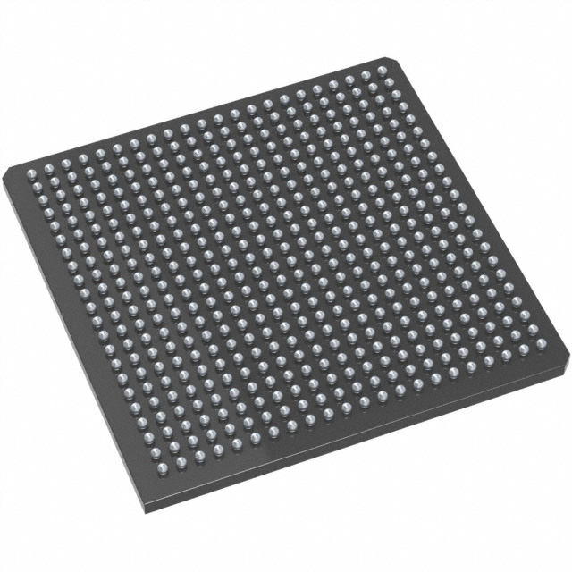
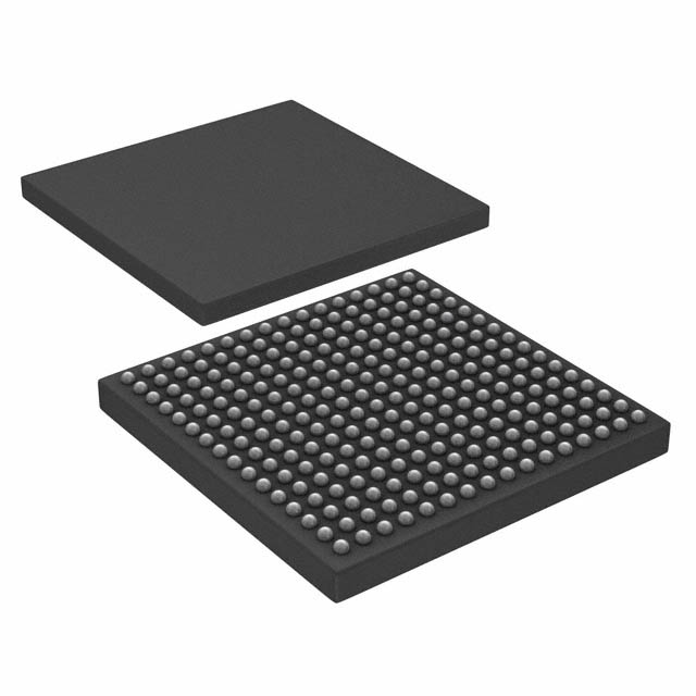
A54SX32A-1FGG484
| Part Description |
SX-A Field Programmable Gate Array (FPGA) IC 249 484-BGA |
|---|---|
| Quantity | 626 Available (as of June 14, 2026) |

| Product Category | Field Programmable Gate Array (FPGA) |
|---|---|
| Manufacturer | Microchip Technology |
| Manufacturing Status | Active |
| Manufacturer Standard Lead Time | 52 Weeks |
| Datasheet |
Specifications & Environmental
| Device Package | 484-FPBGA (27X27) | Grade | Commercial | Operating Temperature | 0°C – 70°C | ||
|---|---|---|---|---|---|---|---|
| Package / Case | 484-BGA | Number of I/O | 249 | Voltage | 2.25 V - 5.25 V | ||
| Mounting Method | Surface Mount | RoHS Compliance | ROHS3 Compliant | REACH Compliance | REACH Unaffected | ||
| Moisture Sensitivity Level | 3 (168 Hours) | Number of LABs/CLBs | 2880 | Number of Logic Elements/Cells | 2880 | ||
| Number of Gates | 48000 | ECCN | 3A991D | HTS Code | 8542.39.0001 | ||
| Qualification | N/A |
Overview of A54SX32A-1FGG484 – SX-A Field Programmable Gate Array (FPGA) IC 249 484-BGA
The A54SX32A-1FGG484 is a commercial-grade, nonvolatile SX-A family FPGA offered in a 484-ball fine-pitch BGA (27 × 27 mm) package. It provides 48,000 system gates and 2,880 logic elements with 249 user-programmable I/O pins, targeting mixed-voltage embedded designs that require a single-chip, configuration-retaining FPGA.
Designed for applications needing deterministic timing, configurable multi-voltage I/O and board-level testability, this device delivers family-level performance characteristics including up to 250 MHz system performance and up to 350 MHz internal performance as documented for the SX-A family.
Key Features
- Logic Capacity — 48,000 system gates and approximately 2,880 logic elements provide mid-range programmable logic density for glue logic, protocol bridging and control functions.
- I/O and Package — 249 user I/Os in a 484-FPBGA (27 × 27) package; surface-mount BGA form factor for compact board-level integration.
- Voltage and Mixed-Voltage Support — Device-level supply range 2.25 V to 5.25 V. SX-A family I/O supports 3.3 V/5 V PCI, 5 V TTL, 3.3 V LVTTL and 2.5 V LVCMOS2 with 5 V input tolerance and 5 V drive capability for mixed-voltage system designs.
- Performance Characteristics — Family-level documented performance includes 250 MHz system performance and 350 MHz internal performance for timing-critical logic.
- Nonvolatile Single-Chip Solution — Nonvolatile architecture retains configuration without external configuration memory, simplifying board design and enabling instant-on behavior.
- System and Board-Level Features — Hot-swap compliant I/Os, power-up/power-down friendly operation (no sequencing required), boundary-scan testing (IEEE 1149.1) and in-system diagnostic/verification capability.
- Security and Reliability — Actel Secure Programming Technology (FuseLock™) to protect design IP and prevent reverse engineering.
- Control and I/O Options — Configurable weak pull-up/pull-down at power-up and individual output slew-rate control to help meet signal-integrity and system-power requirements.
- Environmental and Grade — Commercial grade with an operating temperature range of 0 °C to 70 °C and RoHS-compliant packaging.
- On-Chip Memory — No embedded RAM bits (Total RAM Bits: 0), enabling deterministic flip-flop-based implementations where on-chip RAM is not required.
Typical Applications
- PCI and Bus Interface Logic — 66 MHz PCI compliance and mixed-voltage I/O support make this device suitable for implementing bus bridges, interface logic and custom peripheral controllers.
- Mixed-Voltage System Glue — Configurable I/Os with 5 V tolerance and multi-voltage operation are ideal for level translation, protocol adaptation and board glue between 5 V and lower-voltage subsystems.
- Board-Level Test and Diagnostics — Boundary-scan (JTAG) and in-system diagnostic features support manufacturing test, board bring-up and field verification workflows.
- Secure IP Implementation — Built-in FuseLock programming protects sensitive logic and algorithms implemented in the FPGA.
Unique Advantages
- Nonvolatile, Single-Chip Configuration: Eliminates external configuration memory and simplifies power-up behavior and board design.
- Mixed-Voltage I/O Flexibility: Support for 2.5 V, 3.3 V and 5 V signaling with 5 V tolerance reduces the need for external level shifters in heterogeneous systems.
- Deterministic Timing and High Internal Performance: Documented system and internal performance figures enable predictable timing closure for control and interface logic.
- Production and Diagnostic Friendliness: Boundary-scan and in-system diagnostic capabilities streamline manufacturing test and field troubleshooting.
- IP Protection: FuseLock secure programming protects design confidentiality and reduces risk of reverse engineering.
- Compact BGA Packaging: 484-FPBGA footprint delivers high I/O count in a compact, surface-mount package suitable for dense PCB layouts.
Why Choose A54SX32A-1FGG484?
The A54SX32A-1FGG484 brings SX-A family attributes—nonvolatile configuration, mixed-voltage I/O flexibility and deterministic performance—into a mid-range capacity device with 48,000 system gates and 2,880 logic elements. Its 249 user I/Os and 484-FPBGA package make it a practical choice for embedded designs that require compact form factor, board-level testability and secure in-field configuration retention.
This device is well suited to development teams and procurement looking for a commercial-grade FPGA that balances logic capacity, I/O density and integration features for interface logic, protocol conversion, control functions and secure programmable IP deployment. RoHS-compliant packaging and documented family-level performance add to long-term design predictability and manufacturability.
Request a quote or submit an inquiry to receive pricing, availability and technical support information for A54SX32A-1FGG484.


Date Founded: 1989
Headquarters: Chandler, Arizona, USA
Employees: 22,000+
Revenue: $8.349 Billion
Certifications and Memberships: ISO9001:2015, IATF16949:2016, AS 9100D


