
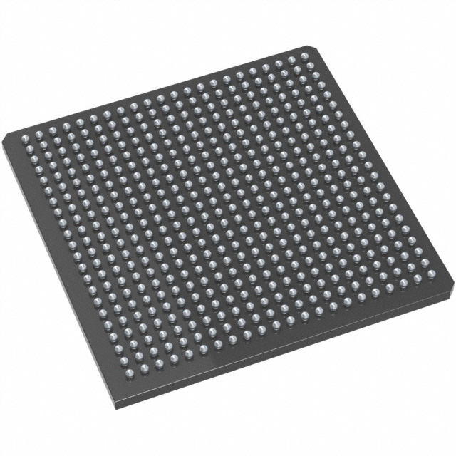
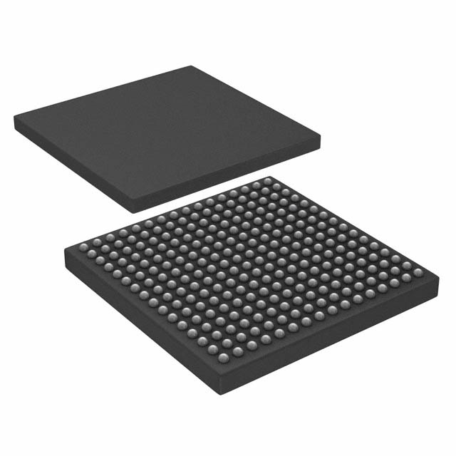
A54SX32A-1FG484
| Part Description |
SX-A Field Programmable Gate Array (FPGA) IC 249 484-BGA |
|---|---|
| Quantity | 1,109 Available (as of June 15, 2026) |
| Product Category | Field Programmable Gate Array (FPGA) |
|---|---|
| Manufacturer | Microchip Technology |
| Manufacturing Status | Active |
| Manufacturer Standard Lead Time | 52 Weeks |
| Datasheet |
Specifications & Environmental
| Device Package | 484-FPBGA (27X27) | Grade | Commercial | Operating Temperature | 0°C – 70°C | ||
|---|---|---|---|---|---|---|---|
| Package / Case | 484-BGA | Number of I/O | 249 | Voltage | 2.25 V - 5.25 V | ||
| Mounting Method | Surface Mount | RoHS Compliance | RoHS non-compliant | REACH Compliance | REACH Unaffected | ||
| Moisture Sensitivity Level | 3 (168 Hours) | Number of LABs/CLBs | 2880 | Number of Logic Elements/Cells | 2880 | ||
| Number of Gates | 48000 | ECCN | 3A991D | HTS Code | 8542.39.0001 | ||
| Qualification | N/A |
Overview of A54SX32A-1FG484 – SX-A Field Programmable Gate Array (FPGA) IC 249 484-BGA
The A54SX32A-1FG484 is a nonvolatile SX-A family FPGA offered by Microchip Technology in a 484-ball fine-pitch BGA package. It provides a mid-range logic capacity with 48,000 system gates, 2,880 logic elements, and 249 user I/O pins, making it suitable for commercial embedded designs that require flexible I/O and reprogrammable logic.
Designed for mixed-voltage systems, the device supports 2.5 V, 3.3 V and 5 V operation with 5 V input tolerance, and operates over a commercial temperature range of 0 °C to 70 °C. The family-level datasheet cites system and internal performance numbers useful for timing-constrained designs.
Key Features
- Logic Capacity Provides 48,000 system gates and 2,880 logic elements (cells), enabling mid-density logic integration on a single device.
- User I/O 249 user-programmable I/O pins with configurable I/O support for 3.3 V/5 V PCI, 5 V TTL, 3.3 V LVTTL and 2.5 V LVCMOS2 signaling, plus 5 V input tolerance and 5 V drive strength.
- Performance Family-level performance cited at up to 250 MHz system performance and up to 350 MHz internal performance for timing-critical partitions.
- Nonvolatile Single-Chip Solution On-chip nonvolatile configuration removes the need for external configuration memory and simplifies system power-up behavior.
- Power and I/O Handling Hot-swap compliant I/Os and power-up/power-down friendly behavior with no sequencing required for supply voltages.
- Security and Test Includes Actel Secure Programming Technology with FuseLock™ to protect design IP and supports IEEE 1149.1 boundary-scan (JTAG) for board-level testability.
- Package and Mounting 484-FPBGA (27 × 27 mm) fine-pitch BGA package, surface-mount mounting for high-density board layouts.
- Voltage and Temperature Supply voltage range of 2.25 V to 5.25 V and commercial operating temperature range of 0 °C to 70 °C.
- Standards Support Family-level support for 66 MHz PCI signaling for card- and bus-level interface applications.
- RoHS Compliance Device and packaging are RoHS compliant.
Typical Applications
- Embedded Control Implement control logic, state machines and protocol handling where a nonvolatile, reprogrammable FPGA simplifies board design and reduces external components.
- I/O Aggregation and Level Translation Aggregate multiple peripheral interfaces and bridge mixed-voltage domains using the device's configurable I/O and 5 V tolerance.
- PCI and Card-Level Interfaces Use in 66 MHz PCI-compliant designs requiring programmable logic and flexible I/O mapping.
- In-System Diagnostics and Test Leverage built-in boundary-scan and in-system diagnostic features for board-level verification and maintenance.
Unique Advantages
- Nonvolatile Configuration: Eliminates the need for external configuration memory and streamlines system boot without additional components.
- Flexible Mixed-Voltage I/O: Configurable I/O standards and 5 V tolerance allow direct interfacing with a wide range of legacy and modern peripherals.
- Integrated Security: FuseLock™ secure programming technology protects intellectual property and prevents unauthorized readback.
- Testability and Diagnostics: IEEE 1149.1 boundary-scan support and in-system diagnostic capabilities help reduce board bring-up time and simplify field troubleshooting.
- Compact, High-Density Package: 484-FPBGA fine-pitch BGA enables a high I/O count in a compact footprint for space-constrained designs.
- Commercial-Grade Reliability: Designed and specified for commercial temperature operation (0 °C to 70 °C) with a broad supply range (2.25–5.25 V) for typical commercial environments.
Why Choose A54SX32A-1FG484?
The A54SX32A-1FG484 positions itself as a versatile, mid-density nonvolatile FPGA for commercial embedded systems that need configurable logic, broad I/O flexibility and secure in-field programmability. With 48,000 system gates, 2,880 logic elements and 249 user I/Os in a fine-pitch 484-BGA package, it balances integration density and board-level I/O capability.
Choose this device for designs that require mixed-voltage interfacing, on-chip nonvolatile configuration and built-in test and security features—delivering a compact solution that reduces BOM complexity while supporting robust system-level diagnostics and programming protection.
Request a quote or contact sales to discuss availability, pricing and how the A54SX32A-1FG484 can fit your next commercial FPGA design.


Date Founded: 1989
Headquarters: Chandler, Arizona, USA
Employees: 22,000+
Revenue: $8.349 Billion
Certifications and Memberships: ISO9001:2015, IATF16949:2016, AS 9100D


