
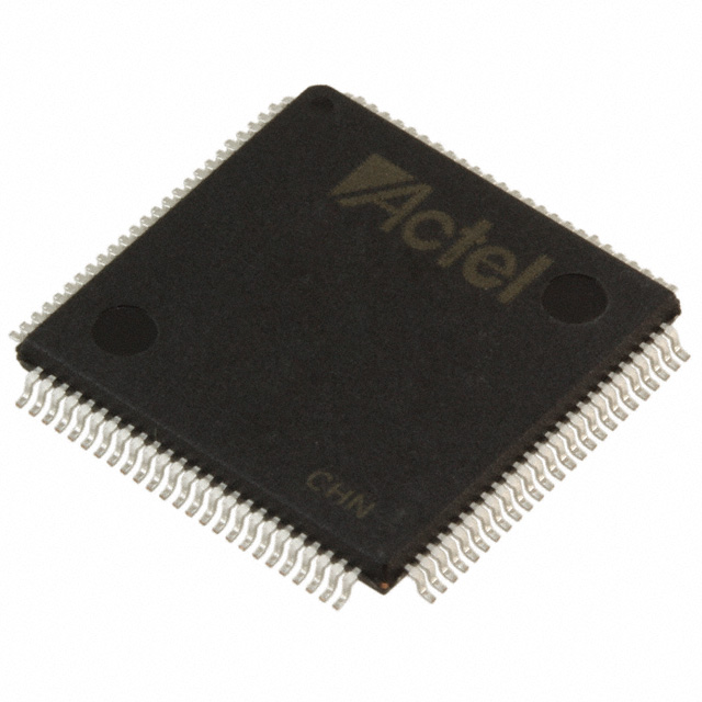
A54SX32A-FTQ100
| Part Description |
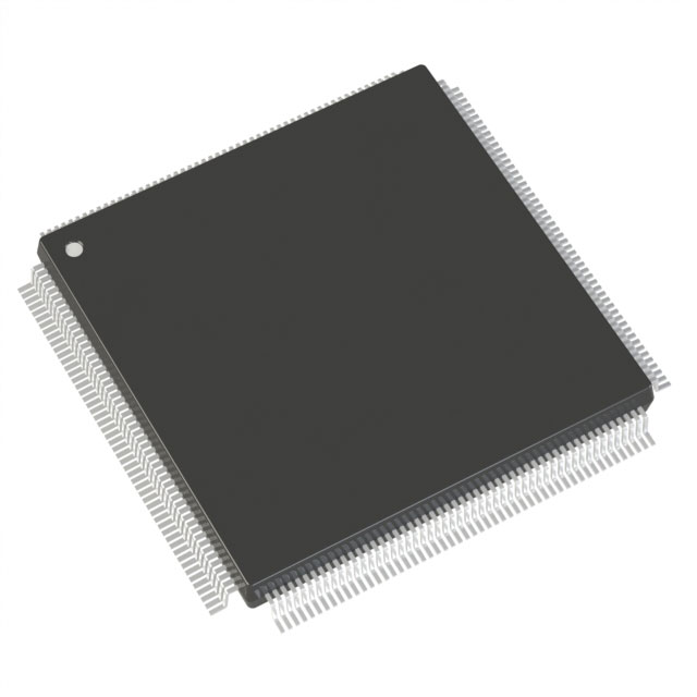
SX-A Field Programmable Gate Array (FPGA) IC 81 100-LQFP |
|---|---|
| Quantity | 703 Available (as of June 18, 2026) |
| Product Category | Field Programmable Gate Array (FPGA) |
|---|---|
| Manufacturer | Microchip Technology |
| Manufacturing Status | Obsolete |
| Manufacturer Standard Lead Time | Contact Us |
| Datasheet |
Specifications & Environmental
| Device Package | 100-TQFP (14x14) | Grade | Commercial | Operating Temperature | 0°C – 70°C | ||
|---|---|---|---|---|---|---|---|
| Package / Case | 100-LQFP | Number of I/O | 81 | Voltage | 2.25 V - 5.25 V | ||
| Mounting Method | Surface Mount | RoHS Compliance | RoHS non-compliant | REACH Compliance | REACH Unaffected | ||
| Moisture Sensitivity Level | 3 (168 Hours) | Number of LABs/CLBs | 2880 | Number of Logic Elements/Cells | 2880 | ||
| Number of Gates | 48000 | ECCN | 3A991D | HTS Code | 8542.39.0001 | ||
| Qualification | N/A |
Overview of A54SX32A-FTQ100 – SX-A Field Programmable Gate Array (FPGA) IC 81 100-LQFP
The A54SX32A-FTQ100 is a commercial-grade SX-A family FPGA offered in a 100-pin LQFP surface-mount package. It delivers a nonvolatile, single-chip FPGA solution with 48,000 system gates and 2,880 logic elements for mid-density programmable logic requirements.
Designed for commercial embedded and interface applications, this device provides flexible I/O support, mixed-voltage operation, JTAG boundary-scan, and family-level performance characteristics such as 250 MHz system performance and 350 MHz internal performance as documented for the SX-A family.
Key Features
- Logic Capacity — 48,000 system gates and approximately 2,880 logic elements, providing a mid-range programmable fabric for glue logic, protocol bridging, and control tasks.
- User I/O — 81 user I/Os available in the 100-pin package to support multiple external interfaces and board-level connectivity.
- Nonvolatile Single-Chip — SX-A family single-chip, nonvolatile architecture simplifies system design by eliminating the need for external configuration memory.
- Mixed-Voltage I/O — Configurable I/O support including 3.3 V / 5 V PCI, 5 V TTL, 3.3 V LVTTL, and 2.5 V LVCMOS2; supports 2.5 V, 3.3 V, and 5 V mixed-voltage operation with 5 V input tolerance and 5 V drive strength.
- Power-Friendly I/Os — Hot-swap compliant I/Os and power-up/power-down friendly behavior with no supply sequencing required, easing integration into multi-rail systems.
- Performance and Timing — Family-documented performance targets include 250 MHz system performance and 350 MHz internal performance; deterministic, user-controllable timing enables predictable design closure.
- System Diagnostics & Test — Boundary-scan testing compliant with IEEE 1149.1 (JTAG) and in-system diagnostic/verification capability via Silicon Explorer II.
- Security — Actel Secure Programming Technology with FuseLock™ to protect bitstream confidentiality and prevent reverse engineering.
- I/O Control — Configurable weak-resistor pull-up or pull-down at power-up and individual output slew-rate control for signal integrity tuning.
- Package & Mounting — 100-LQFP package case (surface mount); supplier device package listed as 100-TQFP (14×14).
- Electrical & Environmental — Supply voltage range 2.25 V to 5.25 V, operating temperature 0 °C to 70 °C, and RoHS compliant.
- Resource Utilization — Supports up to 100% resource utilization and 100% pin locking for deterministic implementation and pin assignment control.
Typical Applications
- Embedded Control and Glue Logic — Implement control-state machines, signal conditioning, and board-level interfacing where mid-range logic capacity and flexible I/O are required.
- Bus and Protocol Bridging — Use the device’s mixed-voltage I/O and PCI-capable features for bridging between different bus standards and voltage domains.
- Prototyping and Development — Single-chip nonvolatile configuration and family tools for in-system diagnostics make the device suitable for rapid prototyping and functional validation.
- Commercial Electronic Systems — Integrate into consumer and commercial products requiring a commercial-grade FPGA with predictable timing and configurable I/O behavior.
Unique Advantages
- Nonvolatile, single-chip solution: Eliminates external configuration components, reducing BOM complexity and board area.
- Flexible mixed-voltage I/O: Simplifies interfacing across 2.5 V, 3.3 V, and 5 V domains with 5 V input tolerance and configurable I/O standards.
- Power-up/down friendly I/Os: No supply sequencing required and hot-swap compliant I/Os reduce integration risk in multi-rail systems.
- Deterministic timing and full resource utilization: User-controllable timing and support for up to 100% utilization enable predictable synthesis and placement outcomes.
- Security and testability: FuseLock secure programming and IEEE 1149.1 boundary-scan facilitate IP protection and production test.
- Commercial operating range and compliance: Designed for 0 °C to 70 °C operation with RoHS compliance for standard commercial product deployments.
Why Choose A54SX32A-FTQ100?
The A54SX32A-FTQ100 positions itself as a practical mid-density FPGA for commercial embedded designs that need a nonvolatile, single-chip programmable solution. With 48,000 system gates, 2,880 logic elements, and 81 user I/Os in a compact 100-pin LQFP package, it balances integration density with flexible I/O and power-friendly behavior.
This device is a fit for engineering teams seeking predictable timing, mixed-voltage interfacing, and on-board security features while keeping the board-level BOM and configuration complexity low. Its RoHS compliance and defined commercial temperature range make it suitable for a broad set of commercial electronic products.
Request a quote or submit a product inquiry to obtain pricing, availability, and ordering information for the A54SX32A-FTQ100.


Date Founded: 1989
Headquarters: Chandler, Arizona, USA
Employees: 22,000+
Revenue: $8.349 Billion
Certifications and Memberships: ISO9001:2015, IATF16949:2016, AS 9100D


