
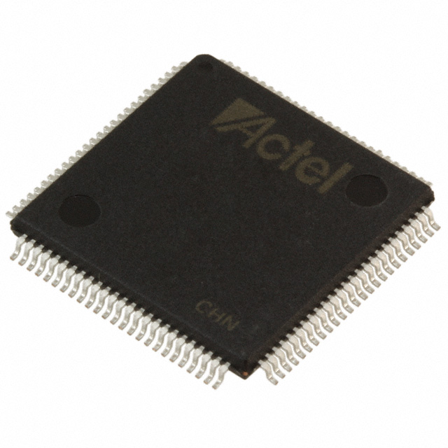
A54SX32A-PQ208I
| Part Description |
SX-A Field Programmable Gate Array (FPGA) IC 174 208-BFQFP |
|---|---|
| Quantity | 74 Available (as of June 15, 2026) |

| Product Category | Field Programmable Gate Array (FPGA) |
|---|---|
| Manufacturer | Microchip Technology |
| Manufacturing Status | Obsolete |
| Manufacturer Standard Lead Time | Contact Us |
| Datasheet |
Specifications & Environmental
| Device Package | 208-PQFP (28x28) | Grade | Industrial | Operating Temperature | -40°C – 85°C | ||
|---|---|---|---|---|---|---|---|
| Package / Case | 208-BFQFP | Number of I/O | 174 | Voltage | 2.25 V - 5.25 V | ||
| Mounting Method | Surface Mount | RoHS Compliance | RoHS non-compliant | REACH Compliance | REACH Unaffected | ||
| Moisture Sensitivity Level | 3 (168 Hours) | Number of LABs/CLBs | 2880 | Number of Logic Elements/Cells | 2880 | ||
| Number of Gates | 48000 | ECCN | 3A991D | HTS Code | 8542.39.0001 | ||
| Qualification | N/A |
Overview of A54SX32A-PQ208I – SX-A Field Programmable Gate Array (FPGA) IC 174 I/O 208-BFQFP
The A54SX32A-PQ208I is a Microchip Technology SX-A family FPGA — a nonvolatile, single-chip programmable logic device designed for mid-density applications. It combines approximately 48,000 system gates and 2,880 logic elements with 174 user-programmable I/O pins to enable flexible interfacing and control in industrial embedded systems.
Built with features such as hot-swap capable I/Os, configurable I/O standards and power-up/power-down friendly operation, the device targets designs that require deterministic timing, in-system diagnostics and reliable configuration without external volatile memory.
Key Features
- Core performance Specified system performance up to 250 MHz and internal performance up to 350 MHz as documented for the SX-A family.
- Logic capacity Approximately 48,000 system gates implemented across 2,880 logic elements, supporting up to 2,012 dedicated flip-flops (family data).
- User I/O 174 user-programmable I/O pins with configurable I/O support for multiple voltage standards (examples in family documentation include 3.3 V/5 V PCI, 5 V TTL, 3.3 V LVTTL, 2.5 V LVCMOS2).
- Nonvolatile single-chip configuration Single-chip, nonvolatile architecture removes the need for external configuration memory and supports secure programming technology (FuseLock™ in family documentation).
- Power and I/O robustness Hot-swap compliant I/Os, power-up/power-down friendly operation (no supply sequencing required) and configurable weak pull-up/pull-down on I/O at power-up (family features).
- Voltage and temperature Wide supply voltage range of 2.25 V to 5.25 V and industrial temperature grade operation from −40 °C to +85 °C.
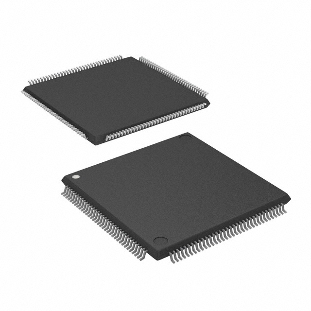
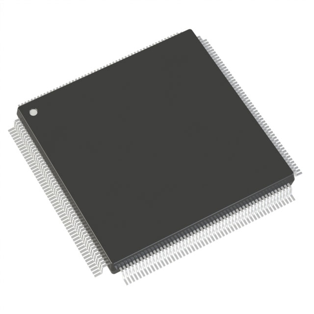
- Package 208-pin BFQFP package case (supplier device package: 208-PQFP 28×28) for board-level integration.
- System testability and security Boundary-scan testing compliant with IEEE 1149.1 (JTAG) and in-system diagnostic/verification capabilities described for the SX-A family.
Typical Applications
- PCI and legacy interface bridging Configurable I/O voltage support and family-level 66 MHz PCI compliance make the device suitable for designs that require mixed-voltage interface translation and protocol bridging.
- Industrial control and automation Industrial temperature rating (−40 °C to +85 °C) and hot-swap capable I/Os support deployment in embedded controllers and fielded automation equipment.
- In-system diagnostics and test environments Built-in boundary-scan (IEEE 1149.1) and family-level in-system diagnostic features assist board-level testing and on-site verification.
Unique Advantages
- Nonvolatile, single-chip FPGA: Eliminates the need for external configuration memory, simplifying BOM and boot architecture.
- Flexible I/O voltage support: Supports multiple logic standards and a wide supply range (2.25 V–5.25 V), enabling mixed-voltage system interfacing.
- Industrial-ready temperature range: Rated for −40 °C to +85 °C, suitable for industrial embedded deployments.
- Significant mid-range capacity: ~48,000 system gates and 2,880 logic elements provide substantial logic resources for control, glue logic and interface tasks.
- Design verification and security: Boundary-scan support and secure programming technology (family feature) help protect IP and accelerate bring-up and test.
Why Choose A54SX32A-PQ208I?
The A54SX32A-PQ208I positions as a robust mid-density, nonvolatile FPGA option for engineers needing stable, in-field configuration, flexible mixed-voltage I/O and industrial temperature operation. Its combination of ~48k gates, 2,880 logic elements and 174 I/Os delivers a balance of capacity and interfacing capability for embedded control, protocol bridging and test-focused designs.
With family-level features such as hot-swap I/Os, deterministic timing behavior, boundary-scan and secure programming, this device supports scalable, reliable designs where in-system diagnostics, configuration security and simplified hardware architecture are important.
If you would like pricing, availability or to request a quote for A54SX32A-PQ208I, submit an inquiry or request a quote through your purchasing channel. Our team can provide lead time and ordering information.


Date Founded: 1989
Headquarters: Chandler, Arizona, USA
Employees: 22,000+
Revenue: $8.349 Billion
Certifications and Memberships: ISO9001:2015, IATF16949:2016, AS 9100D


