
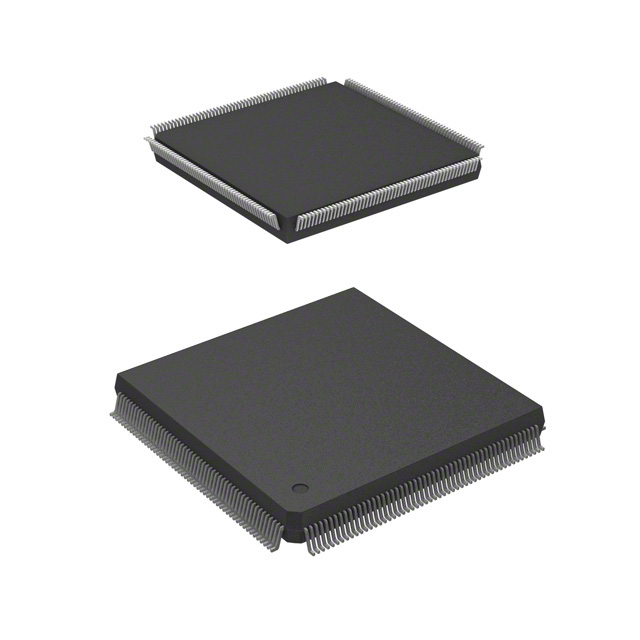
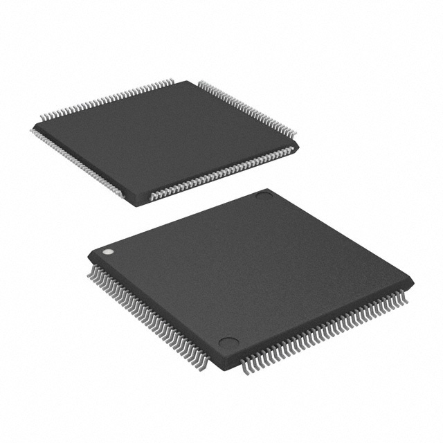
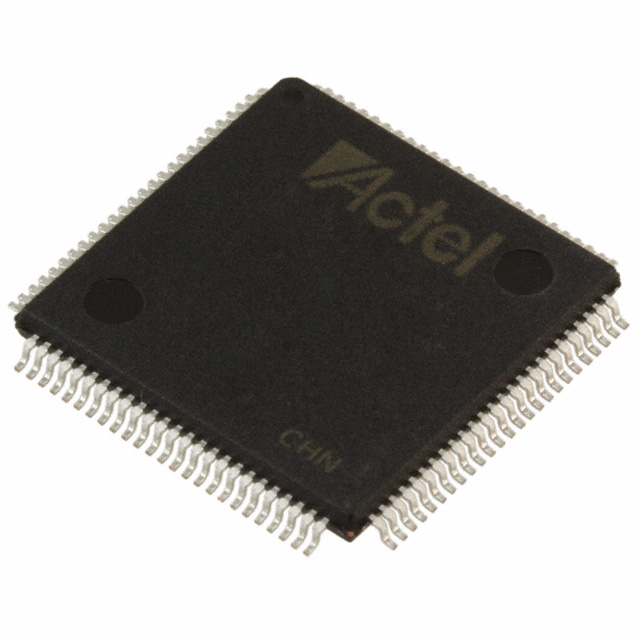
A54SX32A-TQG144I
| Part Description |
SX-A Field Programmable Gate Array (FPGA) IC 113 144-LQFP |
|---|---|
| Quantity | 532 Available (as of June 14, 2026) |

| Product Category | Field Programmable Gate Array (FPGA) |
|---|---|
| Manufacturer | Microchip Technology |
| Manufacturing Status | Active |
| Manufacturer Standard Lead Time | 12 Weeks |
| Datasheet |
Specifications & Environmental
| Device Package | 144-TQFP (20x20) | Grade | Industrial | Operating Temperature | -40°C – 85°C | ||
|---|---|---|---|---|---|---|---|
| Package / Case | 144-LQFP | Number of I/O | 113 | Voltage | 2.25 V - 5.25 V | ||
| Mounting Method | Surface Mount | RoHS Compliance | ROHS3 Compliant | REACH Compliance | REACH Unaffected | ||
| Moisture Sensitivity Level | 3 (168 Hours) | Number of LABs/CLBs | 2880 | Number of Logic Elements/Cells | 2880 | ||
| Number of Gates | 48000 | ECCN | 3A991D | HTS Code | 8542.39.0001 | ||
| Qualification | N/A |
Overview of A54SX32A-TQG144I – SX-A Field Programmable Gate Array (FPGA) IC 113 144-LQFP
The A54SX32A-TQG144I is an SX-A family Field Programmable Gate Array (FPGA) supplied in a 144-pin LQFP surface-mount package. It provides a nonvolatile, single-chip FPGA fabric with 48,000 system gates and 2,880 logic elements, designed for embedded logic, I/O interfacing and control in industrial-grade applications.
Series-level performance characteristics include up to 250 MHz system performance and 350 MHz internal performance. The device targets applications that require mixed-voltage I/O flexibility, deterministic timing and on-board nonvolatile configuration.
Key Features
- Logic Capacity — 48,000 system gates and approximately 2,880 logic elements for implementing medium-complexity custom logic and glue-logic functions.
- User I/O — 113 user-programmable I/O pins enabling flexible interfacing to external peripherals and buses.
- Performance — Series-level documented performance up to 250 MHz system performance and 350 MHz internal performance for timing-critical designs.
- Nonvolatile Single-Chip Architecture — On-chip nonvolatile configuration eliminates the need for external configuration memory and simplifies power-up behavior.
- Configurable I/O Voltage Support — Series-level support for multiple I/O standards (including 2.5 V, 3.3 V and 5 V families) and 5 V input tolerance to accommodate mixed-voltage systems; overall device supply range is 2.25 V to 5.25 V.
- Industrial Temperature Grade — Rated for operation from –40 °C to 85 °C for reliability in industrial environments.
- System-Level Features — Boundary-scan (JTAG) support for test and in-system programming, and series-level in-system diagnostic/verification capability.
- Package and Mounting — 144-LQFP surface-mount package suitable for compact board layouts and automated assembly.
- RoHS Compliant — Manufactured in accordance with RoHS requirements.
Typical Applications
- Industrial Control — Implement custom control logic, I/O aggregation and protocol bridging in factory automation and process-control equipment.
- Embedded System Glue Logic — Replace discrete logic with a compact FPGA to consolidate interfaces, timers and state machines on a single device.
- Mixed-Voltage I/O Interfacing — Interface 2.5 V, 3.3 V and 5 V peripherals with configurable I/O support and 5 V input tolerance.
- Board-Level Test and Diagnostics — Use built-in boundary-scan/JTAG and in-system diagnostic features for manufacturing test and field verification.
Unique Advantages
- Compact, Nonvolatile FPGA: Single-chip nonvolatile configuration removes the need for external configuration memory, reducing BOM and simplifying system power-up.
- Flexible I/O and Supply Range: Wide supply range (2.25 V–5.25 V) and series-level configurable I/O enable mixed-voltage system designs and accommodate diverse peripheral standards.
- Industrial Reliability: Industrial temperature rating (–40 °C to 85 °C) and surface-mount 144-LQFP packaging support deployment in industrial environments.
- Deterministic Performance: Series-level deterministic timing and documented system/internal performance figures support timing-critical applications.
- Testability and Security: Boundary-scan support eases board-level test and production diagnostics; series-level secure programming technology provides protection against reverse engineering.
- Optimized I/O Count vs. Logic Density: 113 user I/Os paired with 2,880 logic elements and 48,000 system gates provide a balanced platform for mid-range designs that need both logic and connectivity.
Why Choose A54SX32A-TQG144I?
The A54SX32A-TQG144I combines a nonvolatile FPGA fabric with a balanced mix of logic capacity and user I/Os in a compact 144-LQFP package, making it well suited for embedded and industrial designs that require reliable on-board configuration and mixed-voltage interfacing. Its industrial temperature rating and RoHS compliance support deployment in temperature-challenging and regulatory-conscious environments.
Choose this device when you need a medium-complexity FPGA solution that simplifies system design by consolidating logic, I/O interfacing and configuration into a single, nonvolatile component backed by series-level features for deterministic timing, testability and in-system verification.
Request a quote or submit an inquiry to get pricing and availability for the A54SX32A-TQG144I for your next design.


Date Founded: 1989
Headquarters: Chandler, Arizona, USA
Employees: 22,000+
Revenue: $8.349 Billion
Certifications and Memberships: ISO9001:2015, IATF16949:2016, AS 9100D


