
A54SX72A-1CQ208M
| Part Description |
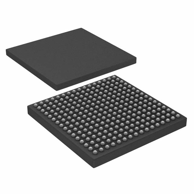
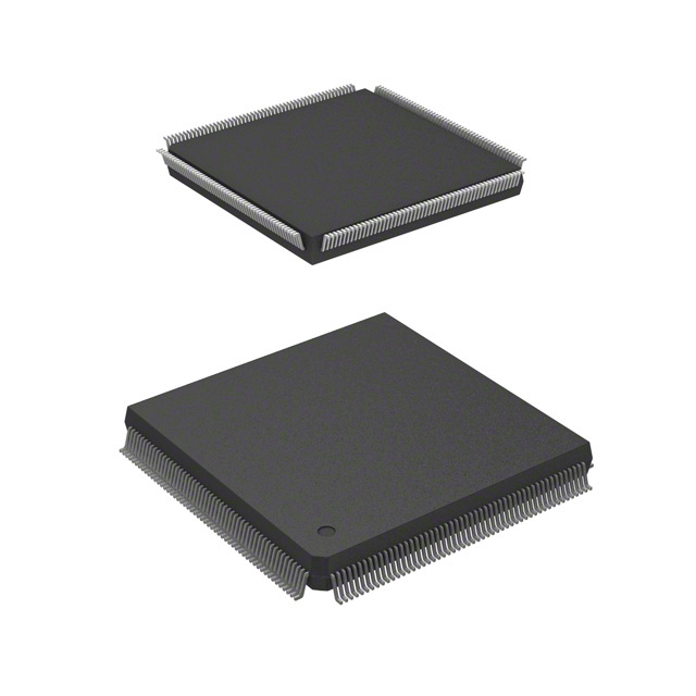
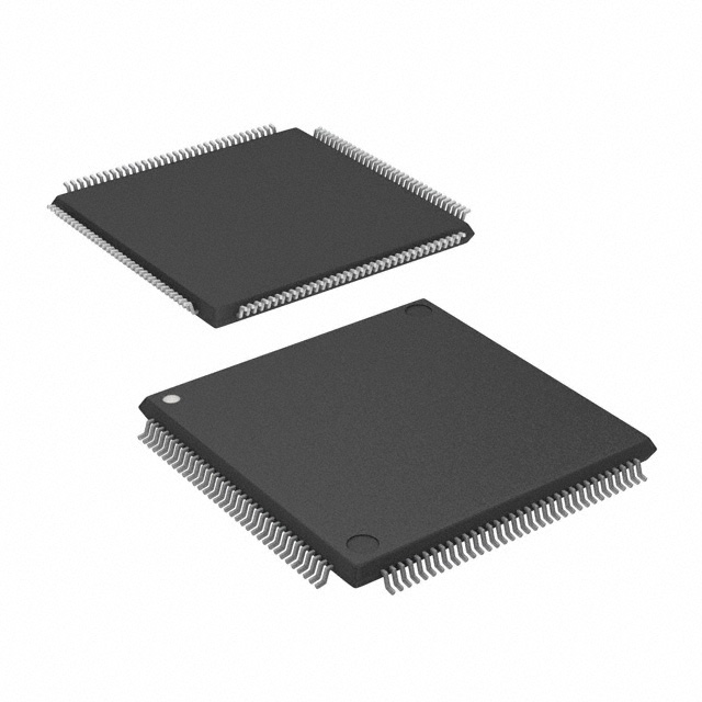
SX-A Field Programmable Gate Array (FPGA) IC 171 208-BFCQFP with Tie Bar |
|---|---|
| Quantity | 275 Available (as of June 15, 2026) |

| Product Category | Field Programmable Gate Array (FPGA) |
|---|---|
| Manufacturer | Microchip Technology |
| Manufacturing Status | Active |
| Manufacturer Standard Lead Time | 44 Weeks |
| Datasheet |
Specifications & Environmental
| Device Package | 208-CQFP (75x75) | Grade | Military | Operating Temperature | -55°C – 125°C | ||
|---|---|---|---|---|---|---|---|
| Package / Case | 208-BFCQFP with Tie Bar | Number of I/O | 171 | Voltage | 2.25 V - 5.25 V | ||
| Mounting Method | Surface Mount | RoHS Compliance | RoHS non-compliant | REACH Compliance | REACH Unaffected | ||
| Moisture Sensitivity Level | 3 (168 Hours) | Number of LABs/CLBs | 6036 | Number of Logic Elements/Cells | 6036 | ||
| Number of Gates | 108000 | ECCN | 3A001A2C | HTS Code | 8542.39.0001 | ||
| Qualification | N/A |
Overview of A54SX72A-1CQ208M – SX-A FPGA, 171 I/O, 208-BFCQFP with Tie Bar
The A54SX72A-1CQ208M is a HiRel SX-A family field programmable gate array (FPGA) in a 208-pin ceramic CQFP package with tie bar, designed and manufactured by Microchip Technology. It delivers a high-density, military-grade programmable logic solution with 108,000 system gates and 6,036 logic elements for complex control, processing and interface functions.
Built for high-reliability environments, this device supports wide voltage operation (2.25 V to 5.25 V), 171 user I/Os, and full military temperature qualification (–55°C to +125°C), making it suitable for applications that require deterministic timing, secure programming and long-term operational stability.
Key Features
- Core Capacity: 108,000 system gates and 6,036 logic elements provide substantial programmable logic resources for medium-to-high complexity designs.
- Flip-Flops and Logic Resources: Up to 2,012 dedicated flip-flops are available to support synchronous logic and state-machine implementation.
- I/O Flexibility: 171 user-programmable I/Os enable extensive peripheral interfacing and board-level integration.
- Performance (family-level): Documented family-level figures include system performance up to 215 MHz (military temperature) and clock-to-out times as low as 5.3 ns (pin-to-pin) under military temperature conditions.
- Voltage and Mixed-Voltage Support: Operates across a wide supply range from 2.25 V to 5.25 V to accommodate mixed-voltage system designs.
- Package: 208-pin ceramic CQFP with tie bar (supplier device package: 208-CQFP (75x75)), designed for surface-mount assembly.
- Military/HiRel Qualification: Military grade device with operating temperature –55°C to +125°C and Class B level production flow and testing as described in the family documentation.
- Security and Reliability (family features): Family-level capabilities include secure programming technology (FuseLock™) and QML certification for traceable high-reliability use.
- Standards Compatibility (family-level): Family documentation references 33 MHz PCI compliance and IEEE 1149.1 boundary-scan (JTAG) support for testability.
- RoHS Compliance: Device is RoHS compliant to meet environmental requirements.
Typical Applications
- Military and Aerospace Systems: Qualified to –55°C to +125°C and produced under a military-grade flow, suitable for avionics, tactical systems and other high-reliability platforms.
- High-Reliability Control and Processing: Uses its 108,000 system gates and 6,036 logic elements for control logic, protocol bridging and real-time data processing in demanding environments.
- Mixed-Voltage Interface Systems: Wide 2.25 V to 5.25 V supply range supports integration in mixed-voltage system topologies and legacy interfaces.
- Secure or IP-Sensitive Designs: Family-level secure programming capabilities support designs that require protection against reverse engineering and unauthorized access.
Unique Advantages
- Military-Grade Qualification: Full military temperature testing and Class B production flow ensure traceable reliability for mission-critical applications.
- Substantial Logic Density: 6,036 logic elements and 108,000 system gates offer the capacity to consolidate functions and reduce BOM in complex systems.
- Broad I/O Count: 171 user I/Os allow flexible connectivity to many peripherals and board-level interfaces without external multiplexing.
- Wide Voltage Range: 2.25 V to 5.25 V operation makes the device adaptable to a variety of supply architectures and mixed-voltage designs.
- Deterministic Timing (family-level): Documented family timing figures and user-controllable timing behavior support predictable, deterministic system performance.
- Manufacturing and Testability: Ceramic CQFP packaging and boundary-scan support enable robust assembly and in-system test capabilities for production environments.
Why Choose A54SX72A-1CQ208M?
The A54SX72A-1CQ208M positions itself as a high-density, military-grade FPGA choice for designers who need reliable, deterministic programmable logic with extensive I/O and a wide operating voltage range. Its 108,000 system gates and 6,036 logic elements offer the headroom to integrate multiple functions on a single device, while family-level features such as secure programming and QML certification address long-term program and security needs.
This device is well suited for organizations developing mission-critical and high-reliability systems that require proven production flows, temperature range assurance and a predictable hardware platform that supports both control and interface consolidation.
Request a quote or submit an inquiry to receive pricing, availability and product lifecycle information for the A54SX72A-1CQ208M.


Date Founded: 1989
Headquarters: Chandler, Arizona, USA
Employees: 22,000+
Revenue: $8.349 Billion
Certifications and Memberships: ISO9001:2015, IATF16949:2016, AS 9100D


