
A54SX72A-1CQ256M
| Part Description |
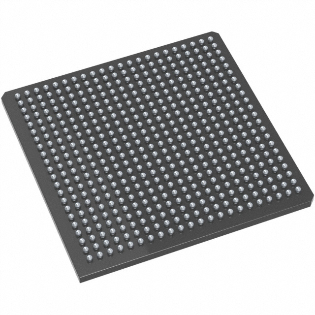
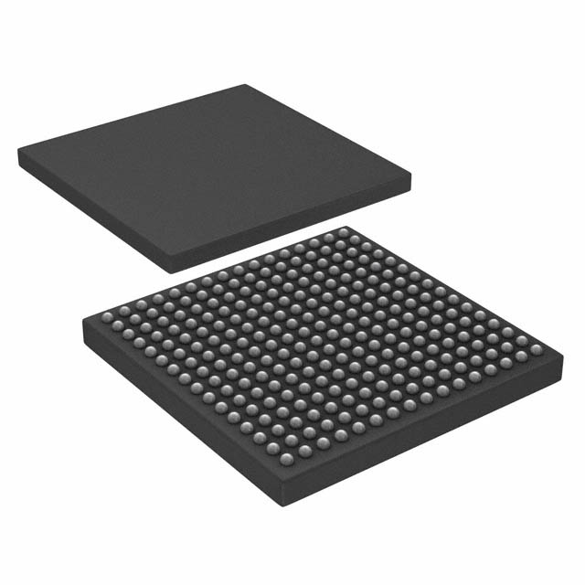
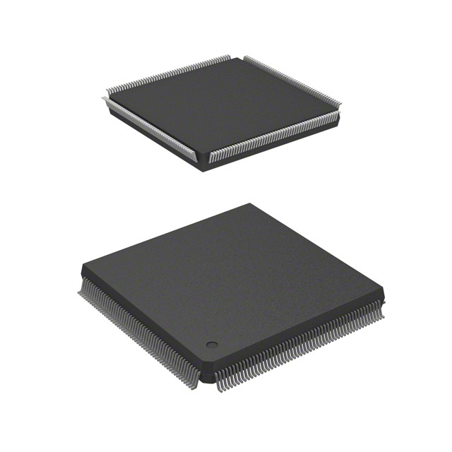
SX-A Field Programmable Gate Array (FPGA) IC 213 256-BFCQFP with Tie Bar |
|---|---|
| Quantity | 448 Available (as of June 18, 2026) |

| Product Category | Field Programmable Gate Array (FPGA) |
|---|---|
| Manufacturer | Microchip Technology |
| Manufacturing Status | Active |
| Manufacturer Standard Lead Time | 44 Weeks |
| Datasheet |
Specifications & Environmental
| Device Package | 256-CQFP (75x75) | Grade | Military | Operating Temperature | -55°C – 125°C | ||
|---|---|---|---|---|---|---|---|
| Package / Case | 256-BFCQFP with Tie Bar | Number of I/O | 213 | Voltage | 2.25 V - 5.25 V | ||
| Mounting Method | Surface Mount | RoHS Compliance | RoHS non-compliant | REACH Compliance | REACH Unaffected | ||
| Moisture Sensitivity Level | 3 (168 Hours) | Number of LABs/CLBs | 6036 | Number of Logic Elements/Cells | 6036 | ||
| Number of Gates | 108000 | ECCN | 3A001A2C | HTS Code | 8542.39.0001 | ||
| Qualification | N/A |
Overview of A54SX72A-1CQ256M – SX-A Field Programmable Gate Array (FPGA) IC 213 256-BFCQFP with Tie Bar
The A54SX72A-1CQ256M is a military-grade SX‑A family FPGA in a 256-pin ceramic CQFP package with tie bar. Designed for high-reliability embedded systems, it provides a dense logic fabric with deterministic timing and a wide operating range for use in harsh environments.
This device targets aerospace, defense and other mission-critical applications that require QML-level screening, extended temperature operation and secure programmable logic with configurable I/O support across multiple voltage domains.
Key Features
- Logic Capacity — 108,000 system gates and 6,036 logic elements provide substantial programmable logic resources for complex functions and system consolidation.
- User I/O — 213 user-programmable I/O pins with configurable support for 3.3 V/5 V PCI, LVTTL and TTL signaling to interface with a broad range of peripherals.
- Timing and Performance — Family-level performance includes up to 215 MHz system performance (military temperature) and 240 MHz internal performance; the A54SX72A device has a documented clock-to-out of 6.7 ns.
- Power and I/O Behavior — Hot-swap compliant I/Os and power-up/power-down friendly operation with no required sequencing for supply voltages.
- Security and Testability — Actel Secure Programming Technology with FuseLock to protect design IP; boundary-scan testing compliant with IEEE 1149.1 (JTAG) for manufacturing diagnostics.
- Reliability and Screening — Military grade with QML certification and 100% military temperature testing (–55°C to +125°C) per device flow; meets MIL-STD-883 product flow screening.
- Voltage and Mounting — Broad supply range from 2.25 V to 5.25 V; surface-mount ceramic 256-BFCQFP package (supplier package: 256-CQFP, 75 × 75).
- Embedded Memory — No embedded RAM bits (Total RAM Bits: 0), enabling deterministic resource planning for external memory needs.
- RoHS Compliance — Device is RoHS compliant.
Typical Applications
- Military and Aerospace Systems — Flight electronics, avionics controllers and mission systems that require QML screening and operation across –55°C to +125°C.
- Secure Embedded Systems — Applications needing hardware IP protection and anti-reverse-engineering measures using FuseLock secure programming.
- High-Reliability Control — Deterministic timing and hot-swap I/O support for redundant control, telemetry and data-acquisition subsystems.
- Boundary-Scan Test Environments — Designs that leverage IEEE 1149.1 JTAG for in-circuit testability and board-level diagnostics.
Unique Advantages
- QML‑level Screening: Designed and tested to military screening flows (MIL-STD-883), supporting deployment in mission-critical environments.
- Secure Programming: FuseLock technology protects design IP and helps prevent reverse engineering.
- Wide Voltage Support: 2.25 V to 5.25 V supply range and 5 V input tolerance on I/Os simplify mixed-voltage system integration.
- High I/O Count: 213 user I/Os enable extensive peripheral interfacing without external glue logic.
- Deterministic, Testable Design: Fixed timing characteristics and IEEE 1149.1 boundary-scan support improve verification and manufacturing yield.
- Military Temperature Tested: 100% tested across –55°C to +125°C for predictable behavior in extreme environments.
Why Choose A54SX72A-1CQ256M?
The A54SX72A-1CQ256M combines a high logic capacity (108,000 system gates, 6,036 logic elements) with military-grade screening and secure programming features, making it suited for designers who need deterministic FPGA performance in harsh or security-sensitive applications. Its 213 I/Os, wide supply range and ceramic CQFP packaging support dense, reliable system-level integration.
For teams building aerospace, defense or other high-reliability systems, this device provides a balance of capacity, proven family-level performance and testability to support long-term deployment and maintainability.
Request a quote or submit a purchasing inquiry to evaluate the A54SX72A-1CQ256M for your next high-reliability FPGA design.


Date Founded: 1989
Headquarters: Chandler, Arizona, USA
Employees: 22,000+
Revenue: $8.349 Billion
Certifications and Memberships: ISO9001:2015, IATF16949:2016, AS 9100D


