
A54SX72A-1FG256
| Part Description |
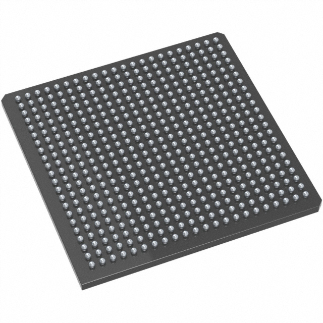
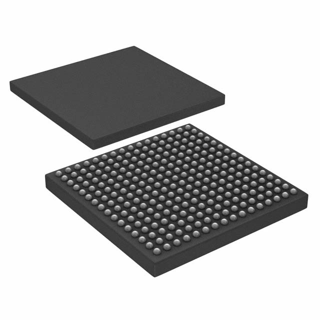
SX-A Field Programmable Gate Array (FPGA) IC 203 256-BGA |
|---|---|
| Quantity | 533 Available (as of June 10, 2026) |

| Product Category | Field Programmable Gate Array (FPGA) |
|---|---|
| Manufacturer | Microchip Technology |
| Manufacturing Status | Active |
| Manufacturer Standard Lead Time | 12 Weeks |
| Datasheet |
Specifications & Environmental
| Device Package | 256-FPBGA (17x17) | Grade | Commercial | Operating Temperature | 0°C – 70°C | ||
|---|---|---|---|---|---|---|---|
| Package / Case | 256-BGA | Number of I/O | 203 | Voltage | 2.25 V - 5.25 V | ||
| Mounting Method | Surface Mount | RoHS Compliance | RoHS non-compliant | REACH Compliance | REACH Unaffected | ||
| Moisture Sensitivity Level | 3 (168 Hours) | Number of LABs/CLBs | 6036 | Number of Logic Elements/Cells | 6036 | ||
| Number of Gates | 108000 | ECCN | 3A991D | HTS Code | 8542.39.0001 | ||
| Qualification | N/A |
Overview of A54SX72A-1FG256 – SX-A Field Programmable Gate Array (FPGA), 203 I/O, 256‑BGA
The A54SX72A-1FG256 is a nonvolatile SX-A family FPGA from Microchip Technology that integrates programmable logic and configurable I/O in a single 256‑ball fine‑pitch BGA package. With 108,000 system gates and 6,036 logic elements, it is intended for designs that require high gate density, flexible I/O support and deterministic timing in a commercially graded device.
This device supports mixed‑voltage operation and a broad supply range, making it suitable for embedded control, interface bridging and system consolidation where a nonvolatile single‑chip solution and in‑system diagnostics are important.
Key Features
- Logic Capacity – 108,000 system gates and 6,036 logic elements with up to 2,012 dedicated flip‑flops for complex logic implementation and register‑rich designs.
- Performance – SX‑A family performance characteristics include up to 250 MHz system performance and up to 350 MHz internal performance as documented for the family.
- Configurable I/O – 203 user‑programmable I/Os on the 256‑BGA package, with configurable support for multiple I/O standards and 5 V tolerance as described in the SX‑A family documentation.
- Voltage and Power – Flexible supply operation from 2.25 V to 5.25 V, enabling mixed‑voltage system integration with power‑up/down friendly behavior (no supply sequencing required).
- Nonvolatile Single‑Chip Solution – Built as a nonvolatile FPGA family member, eliminating need for external configuration memory in deployed systems.
- Security and Test – Includes Actel Secure Programming Technology with FuseLock™ for anti‑reverse engineering protection and supports IEEE 1149.1 (JTAG) boundary‑scan testing for board‑level diagnostics.
- In‑System Diagnostics – Family features include unique in‑system diagnostic and verification capabilities (Silicon Explorer II) to aid validation and field diagnostics.
- Package and Grade – 256‑FBGA (1.0 mm fine‑pitch BGA, 17×17 mm) in a commercial grade device with operating temperature range 0 °C to 70 °C.
- On‑Chip Memory – Total on‑chip RAM reported as 0 bits; this device targets logic‑centric implementations rather than embedded RAM applications.
Typical Applications
- Interface Bridging – Use the configurable I/O and mixed‑voltage support to implement protocol bridging and level translation between subsystems.
- Embedded Control – Consolidate control logic and state machines within the FPGA’s 6,036 logic elements and flip‑flop resources for compact embedded designs.
- PCI‑Capable Systems – SX‑A family documentation includes PCI‑compliant I/O support for 66 MHz PCI applications where a nonvolatile FPGA is required.
- Board Test and Diagnostics – Leverage boundary‑scan (IEEE 1149.1) and in‑system diagnostic features to streamline board‑level test, verification and field diagnostics.
Unique Advantages
- Highly integrated, nonvolatile solution: Single‑chip nonvolatile FPGA removes the need for external configuration memory and simplifies power‑up behavior.
- Flexible I/O and mixed‑voltage operation: 203 configurable I/Os and a wide supply voltage range allow integration with a variety of system I/O standards without extra level‑shifters.
- Deterministic timing and performance: Family performance characteristics and deterministic timing controls support predictable system timing and high‑speed internal paths.
- Security‑oriented programming: FuseLock™ secure programming technology offers protection against reverse engineering and unauthorized access to bitstream contents.
- Built‑in testability: IEEE 1149.1 boundary‑scan and in‑system diagnostics simplify production test and in‑field verification workflows.
- Compact, high‑density packaging: 256‑FBGA fine‑pitch package provides a high I/O count and compact board footprint for space‑constrained designs.
Why Choose A54SX72A-1FG256?
The A54SX72A-1FG256 provides a high‑density, nonvolatile FPGA option for commercial‑grade designs that require comprehensive I/O flexibility, deterministic timing and built‑in security and test features. Its combination of 108,000 system gates, 6,036 logic elements, and 2,012 flip‑flop capacity makes it suitable for consolidating complex glue logic, interface functions and control tasks into a single device.
This part is well suited to product teams seeking a nonvolatile FPGA with family‑level performance characteristics, configurable I/O options and features that support production test and field diagnostics, while operating within a commercial temperature range.
Request a quote or submit an inquiry to discuss availability, pricing and lead times for the A54SX72A-1FG256. Our team can provide additional ordering and supply information tailored to your project needs.


Date Founded: 1989
Headquarters: Chandler, Arizona, USA
Employees: 22,000+
Revenue: $8.349 Billion
Certifications and Memberships: ISO9001:2015, IATF16949:2016, AS 9100D


