
A54SX72A-1FG484I
| Part Description |
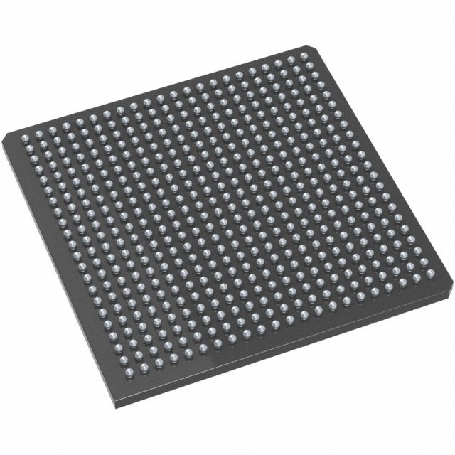
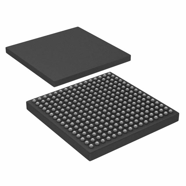
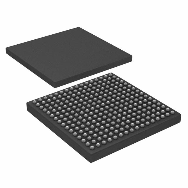
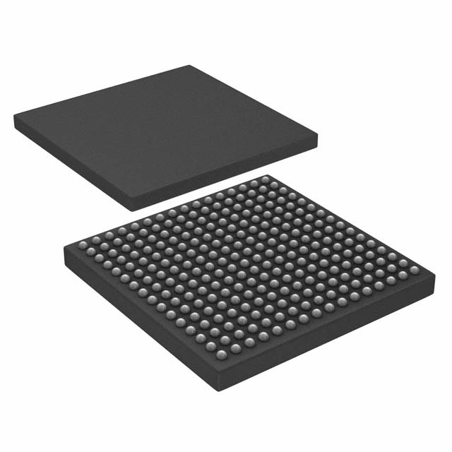
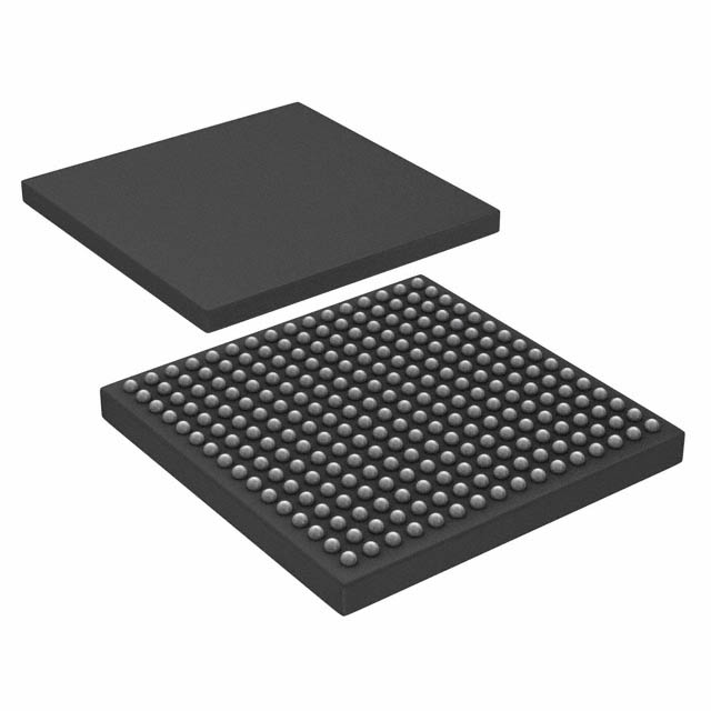
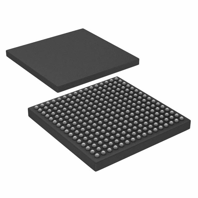
SX-A Field Programmable Gate Array (FPGA) IC 360 484-BGA |
|---|---|
| Quantity | 707 Available (as of October 7, 2026) |
| Product Category | Field Programmable Gate Array (FPGA) |
|---|---|
| Manufacturer | Microchip Technology |
| Manufacturing Status | Active |
| Manufacturer Standard Lead Time | 12 Weeks |
| Datasheet |
Specifications & Environmental
| Device Package | 484-FPBGA (27X27) | Grade | Industrial | Operating Temperature | -40°C – 85°C | ||
|---|---|---|---|---|---|---|---|
| Package / Case | 484-BGA | Number of I/O | 360 | Voltage | 2.25 V - 5.25 V | ||
| Mounting Method | Surface Mount | RoHS Compliance | RoHS non-compliant | REACH Compliance | REACH Unaffected | ||
| Moisture Sensitivity Level | 3 (168 Hours) | Number of LABs/CLBs | 6036 | Number of Logic Elements/Cells | 6036 | ||
| Number of Gates | 108000 | ECCN | 3A991D | HTS Code | 8542.39.0001 | ||
| Qualification | N/A |
Overview of A54SX72A-1FG484I – SX-A Field Programmable Gate Array (FPGA), 108k Gates, 360 I/O, 484-FPBGA
The A54SX72A-1FG484I is an SX-A family nonvolatile FPGA offering 108,000 system gates and 6,036 logic elements in a 484-ball fine-pitch BGA package. Designed for industrial-temperature operation, this device provides a mix of high I/O density (up to 360 user-programmable I/Os), configurable mixed-voltage I/O support, and deterministic timing for embedded and system-level logic implementation.
This single-chip, nonvolatile FPGA is targeted at designs that require substantial gate capacity and flexible I/O signaling across 2.25 V to 5.25 V supply ranges while maintaining industrial temperature range operation (–40 °C to +85 °C).
Key Features
- Core capacity and logic — 108,000 system gates with 6,036 logic elements (combinatorial cells) and up to 2,012 dedicated flip-flops, delivering substantial logic resources for complex designs.
- I/O density and configurability — Up to 360 user-programmable I/Os with configurable support for 3.3 V / 5 V PCI, 5 V TTL, 3.3 V LVTTL and 2.5 V LVCMOS2 signaling; supports mixed-voltage operation with 5 V input tolerance and 5 V drive strength.
- Performance and timing — 250 MHz system performance and up to 350 MHz internal performance with deterministic, user-controllable timing suitable for synchronous system designs.
- Power and reliability — Nonvolatile single-chip architecture; power-up/power-down friendly (no sequencing required for supply voltages) and hot-swap compliant I/Os to support robust power management and board-level integration.
- Package and mounting — 484-FPBGA (27×27) fine-pitch BGA package, surface-mount mounting, optimized for high I/O density and compact board integration.
- Temperature and grade — Industrial temperature grade with operating range from –40 °C to +85 °C.
- Security and test — Support for boundary-scan (IEEE 1149.1) for board-level testing and Actel Secure Programming Technology (FuseLock) to protect bitstream confidentiality and prevent reverse engineering.
- Diagnostics and development — In-system diagnostic and verification capability via Silicon Explorer II (as provided for the SX-A family) to aid debugging and validation.
- Memory — Device reports no embedded RAM bits (Total RAM Bits: 0).
Typical Applications
- Industrial control — Implement custom logic, I/O translation and control functions across a wide operating temperature range with robust, power-friendly I/O behavior.
- High-density I/O systems — Use the 360 user-programmable I/Os for board-level glue logic, protocol bridging, and multi-signal interfacing where mixed-voltage signaling is required.
- PCI-based or legacy interface designs — Integrate with 3.3 V / 5 V PCI signaling and 66 MHz PCI-compliant interfaces where nonvolatile configuration and deterministic timing are needed.
- In-system verification and secure designs — Leverage in-system diagnostics and FuseLock programming to protect intellectual property and simplify field validation.
Unique Advantages
- High gate and logic density: 108,000 system gates and 6,036 logic elements provide ample resources for large finite-state machines, glue logic and control fabrics without external logic expansion.
- Flexible, mixed-voltage I/O: Configurable I/Os that support multiple voltage standards and tolerate 5 V inputs reduce the need for level shifters and simplify board design.
- Nonvolatile, single-chip solution: Eliminates external configuration memory and reduces BOM while providing predictable power-up behavior (no supply sequencing required).
- Industrial-grade operation: Rated for –40 °C to +85 °C and supplied in a compact 484-FPBGA surface-mount package suitable for dense, reliable assemblies.
- Built-in test and security: Boundary-scan support and FuseLock programming help secure designs and accelerate manufacturing test and field diagnostics.
Why Choose A54SX72A-1FG484I?
The A54SX72A-1FG484I combines substantial logic capacity with a high count of configurable I/Os and mixed-voltage support, making it a practical choice for industrial and system-level designs that require nonvolatile configuration and robust power behavior. Its deterministic timing and documented internal performance figures support predictable design closure for synchronous applications.
This device is well suited to engineering teams that need a single-chip FPGA solution with high I/O density, secure programming options, and industrial temperature capability—providing a balance of integration, testability and deployment-ready reliability.
Request a quote or submit a product inquiry to obtain pricing, lead-time and availability information for the A54SX72A-1FG484I.





















Date Founded: 1989
Headquarters: Chandler, Arizona, USA
Employees: 22,000+
Revenue: $8.349 Billion
Certifications and Memberships: ISO9001:2015, IATF16949:2016, AS 9100D




