
A54SX72A-1FGG256M
| Part Description |
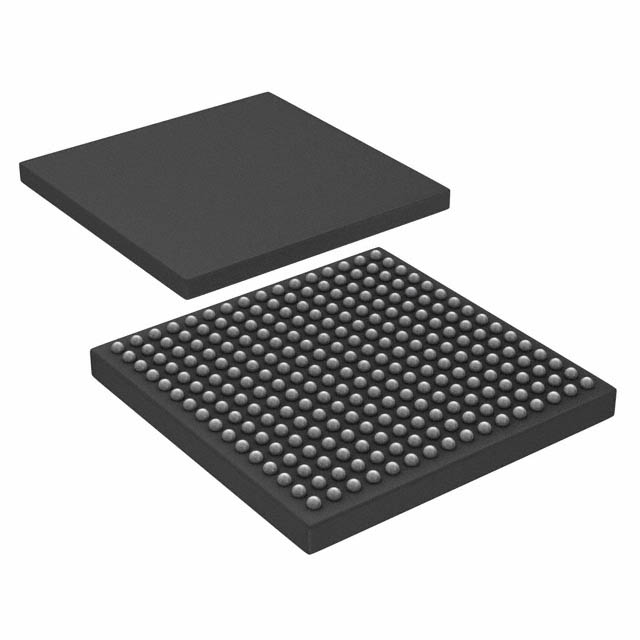
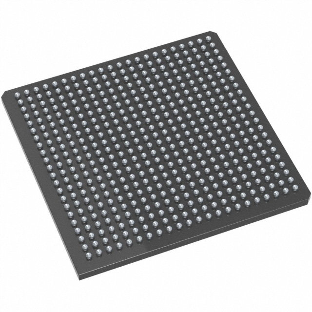
SX-A Field Programmable Gate Array (FPGA) IC 203 256-BGA |
|---|---|
| Quantity | 212 Available (as of June 15, 2026) |
| Product Category | Field Programmable Gate Array (FPGA) |
|---|---|
| Manufacturer | Microchip Technology |
| Manufacturing Status | Active |
| Manufacturer Standard Lead Time | 20 Weeks |
| Datasheet |
Specifications & Environmental
| Device Package | 256-FPBGA (17x17) | Grade | Military | Operating Temperature | -55°C – 125°C | ||
|---|---|---|---|---|---|---|---|
| Package / Case | 256-BGA | Number of I/O | 203 | Voltage | 2.25 V - 5.25 V | ||
| Mounting Method | Surface Mount | RoHS Compliance | ROHS3 Compliant | REACH Compliance | REACH Unaffected | ||
| Moisture Sensitivity Level | 3 (168 Hours) | Number of LABs/CLBs | 6036 | Number of Logic Elements/Cells | 6036 | ||
| Number of Gates | 108000 | ECCN | 3A001A2C | HTS Code | 8542.39.0001 | ||
| Qualification | N/A |
Overview of A54SX72A-1FGG256M – SX-A Field Programmable Gate Array (FPGA) IC 203 256-BGA
The A54SX72A-1FGG256M is an SX-A family FPGA from Microchip Technology designed for high-performance, nonvolatile programmable logic in demanding environments. The device integrates approximately 108,000 system gates and 6,036 logic elements in a 256-pin fine-pitch BGA package, with up to 203 user I/Os and support for mixed-voltage operation.
Targeted at applications that require deterministic timing, secure in-system programming, and wide operating conditions, this military-grade device offers wide supply tolerance and an extended temperature range for robust embedded system designs.
Key Features
- Logic Capacity Approximately 108,000 system gates and 6,036 logic elements provide substantial programmable logic resource for complex glue logic and custom processing functions.
- Flip-Flop Resources Up to 2,012 dedicated flip-flops enable large synchronous designs and state-machine implementations.
- I/O Flexibility 203 user-programmable I/O pins with configurable support for 3.3 V / 5 V PCI, 5 V TTL, 3.3 V LVTTL and 2.5 V LVCMOS2 signals, including 5 V input tolerance and 5 V drive strength.
- Performance Documented system performance up to 250 MHz and internal performance up to 350 MHz for latency-sensitive paths.
- Power and Supply Wide operating supply range from 2.25 V to 5.25 V and power-up/down friendly behavior that requires no sequencing of supply voltages.
- Package and Mounting 256-FPBGA (17×17) fine-pitch BGA, surface-mount package for compact board-level integration.
- Environmental and Grade Military grade device with operating temperature range of −55 °C to +125 °C and RoHS-compliant packaging.
- Security and Test Nonvolatile single‑chip architecture with Actel Secure Programming Technology (FuseLock) and IEEE 1149.1 boundary-scan testing support for IP protection and board-level testability.
- Diagnostics and Verification In-system diagnostic and verification capability via Silicon Explorer II for on-board validation and troubleshooting.
Typical Applications
- Military and Aerospace Systems Military-grade temperature range and rugged supply tolerance make the device suitable for embedded control, signal processing interface logic, and mission-critical subsystems.
- PCI-Based Interfaces Configurable I/O supporting 3.3 V / 5 V PCI levels is useful for implementing PCI-compliant interface logic and bridge functions.
- Secure and Protected Designs FuseLock secure programming supports applications that require protection from reverse engineering and IP theft.
- In-System Diagnostics and Prototyping Built-in in-system verification features enable board bring-up, diagnostics, and iterative hardware validation.
Unique Advantages
- High-density, nonvolatile logic: 108,000 system gates and 6,036 logic elements deliver substantial programmable capacity without external configuration memory.
- Wide I/O and voltage support: 203 user I/Os with mixed-voltage operation and 5 V tolerance/drive simplify interfacing to diverse legacy and modern peripherals.
- Rugged operating envelope: Military grade and −55 °C to +125 °C operating range support deployment in harsh and temperature-extreme environments.
- Deterministic performance: Documented system and internal performance figures enable predictable timing for latency-sensitive designs.
- Integrated security and test: FuseLock programming plus boundary-scan support reduce risk from IP compromise and improve manufacturability and test coverage.
- Single-chip solution: Nonvolatile FPGA architecture eliminates the need for external configuration devices, simplifying BOM and system-level design.
Why Choose A54SX72A-1FGG256M?
The A54SX72A-1FGG256M positions itself as a high-capacity, nonvolatile FPGA option for designs that demand predictable performance, secure programming, and broad I/O flexibility. With approximately 108,000 system gates, 6,036 logic elements, and 203 I/Os in a 256-pin fine-pitch BGA, it addresses complex logic integration while reducing external components.
Its wide supply voltage range, mixed-voltage I/O support, and military-grade temperature rating make it a practical choice for rugged embedded systems, PCI interface logic, and secure applications where long-term robustness and in-system diagnostics are required.
Request a quote or submit an inquiry for pricing and availability for the A54SX72A-1FGG256M.


Date Founded: 1989
Headquarters: Chandler, Arizona, USA
Employees: 22,000+
Revenue: $8.349 Billion
Certifications and Memberships: ISO9001:2015, IATF16949:2016, AS 9100D


