
AGLN060V2-ZVQ100
| Part Description |
IGLOO nano Field Programmable Gate Array (FPGA) IC 71 18432 1536 100-TQFP |
|---|---|
| Quantity | 1,571 Available (as of June 9, 2026) |

| Product Category | Field Programmable Gate Array (FPGA) |
|---|---|
| Manufacturer | Microchip Technology |
| Manufacturing Status | Obsolete |
| Manufacturer Standard Lead Time | Contact Us |
| Datasheet |
Specifications & Environmental
| Device Package | 100-VQFP (14x14) | Grade | Commercial | Operating Temperature | -20°C – 85°C | ||
|---|---|---|---|---|---|---|---|
| Package / Case | 100-TQFP | Number of I/O | 71 | Voltage | 1.14 V - 1.575 V | ||
| Mounting Method | Surface Mount | RoHS Compliance | RoHS non-compliant | REACH Compliance | REACH Unaffected | ||
| Moisture Sensitivity Level | 3 (168 Hours) | Number of LABs/CLBs | 1536 | Number of Logic Elements/Cells | 1536 | ||
| Number of Gates | 60000 | ECCN | 3A991D | HTS Code | 8542.39.0001 | ||
| Qualification | N/A | Total RAM Bits | 18432 |
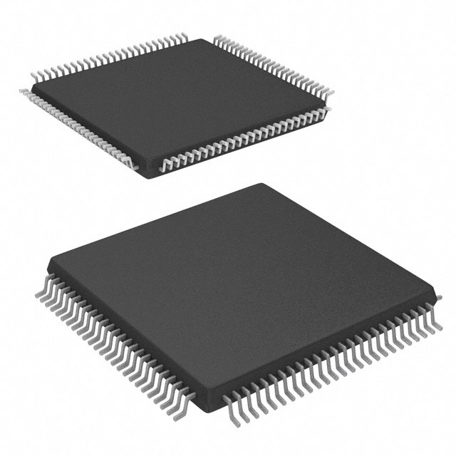
Overview of AGLN060V2-ZVQ100 – IGLOO nano FPGA, 1536 logic elements, 71 I/Os, 100-TQFP
The AGLN060V2-ZVQ100 is an IGLOO nano low-power flash Field Programmable Gate Array (FPGA) from Microchip Technology. It combines flash-based reprogrammability, on-chip embedded memory, and mixed-voltage I/O capability in a compact 100-pin TQFP package for space-constrained commercial designs.
Targeted at low-power and mixed-voltage embedded applications, this device delivers 60,000 system gates, 1,536 logic elements, approximately 18 kbits of on-chip RAM, and up to 71 user I/Os while supporting single-voltage operation and commercial temperature ranges.
Key Features
- Core & Logic — 60,000 system gates and 1,536 logic elements provide a programmable fabric suitable for control, glue logic, and mid-density FPGA tasks.
- Embedded Memory — Approximately 18 kbits of on-chip SRAM arranged in 4,608-bit block structures and 1 kbit of FlashROM user nonvolatile memory for compact data storage and state retention.
- Low-Power Operation — Flash-based architecture with Flash*Freeze technology (series feature) enables ultra-low power retention of FPGA content; device supports a core/I/O voltage supply range of 1.14 V to 1.575 V for low-voltage systems.
- Secure In-System Programming — On-chip 128-bit AES decryption for in-system programming via JTAG (IEEE 1532–compliant) and FlashLock® support for secure device configuration.
- Advanced I/Os — Up to 71 user I/Os with bank-selectable voltages and mixed-voltage support (1.2 V, 1.5 V, 1.8 V, 2.5 V, 3.3 V), selectable input features, and programmable output drive/slew options.
- Clocking and Timing — Configurable Clock Conditioning Circuit (CCC) blocks with an integrated PLL option provide flexible clock multiply/divide and phase-shift capabilities (series-level feature).
- Package & Mounting — 100-pin TQFP (100-VQFP, 14×14 mm footprint) surface-mount package designed for standard PCB assembly; commercial-grade operating range from -20°C to +85°C.
- Reprogrammable Flash Technology — Flash-based CMOS process retains programmed design when powered off and supports instant-on operation (series feature).
Typical Applications
- Low-Power Embedded Control — Ideal for battery-powered or always-on controllers where Flash*Freeze and low-voltage operation reduce standby and active power.
- Mixed-Voltage Interface Bridging — Bank-selectable I/O voltages and up to 71 user I/Os simplify interfacing between 1.2 V–3.3 V domains in compact systems.
- Secure Configuration — Designs that require secure in-system programming and encrypted configuration benefit from on-chip 128-bit AES decryption and FlashLock® features.
- Compact Programmable Logic — Suitable for glue logic, protocol adaptation, and peripheral control in compact commercial electronic products thanks to the 100-TQFP footprint and on-chip SRAM.
Unique Advantages
- Low-power retention with Flash*Freeze: Allows the FPGA to maintain configuration with ultra-low standby power, reducing system power budgets.
- Integrated security for in-field updates: On-chip AES decryption for JTAG-based ISP provides a secure mechanism for updating device configuration in-system.
- Mixed-voltage flexibility: Bank-selectable I/O voltages and a wide supported voltage range enable straightforward integration with multiple logic families and peripheral voltages.
- Compact, surface-mount package: 100-pin TQFP (14×14 mm) offers a small footprint for space-constrained boards while providing up to 71 user I/Os.
- Nonvolatile, instant-on operation: Flash-based architecture retains design when powered off and supports rapid start-up behavior at system power-up.
Why Choose AGLN060V2-ZVQ100?
The AGLN060V2-ZVQ100 positions itself as a compact, low-power, flash-reprogrammable FPGA for commercial embedded systems that require moderate logic capacity, mixed-voltage interfacing, and secure in-field programmability. With 60,000 system gates, 1,536 logic elements, approximately 18 kbits of embedded SRAM, and up to 71 I/Os in a 100-TQFP package, it balances integration and board-space efficiency for a wide range of designs.
Choose this device for applications that prioritize low standby power, secure configuration management, and flexible I/O voltage support within a commercial temperature range. Its flash-based nonvolatile configuration and integrated clocking and security features help simplify system design and long-term maintainability.
Request a quote or submit an inquiry to obtain pricing and availability for AGLN060V2-ZVQ100.


Date Founded: 1989
Headquarters: Chandler, Arizona, USA
Employees: 22,000+
Revenue: $8.349 Billion
Certifications and Memberships: ISO9001:2015, IATF16949:2016, AS 9100D


