
AGLN125V5-ZVQ100
| Part Description |
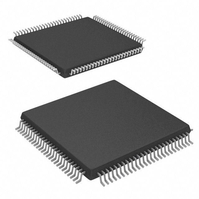
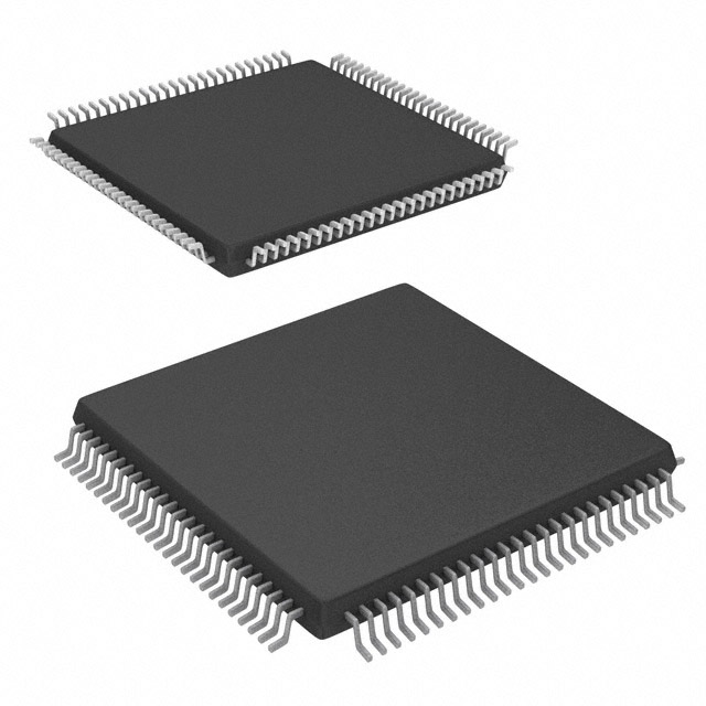
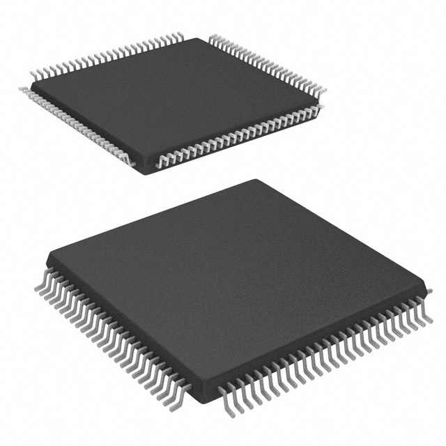
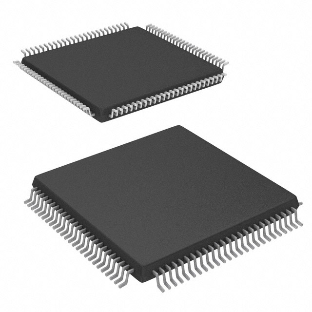
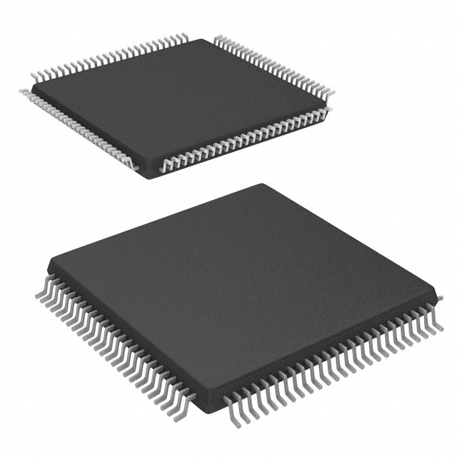
IGLOO nano Field Programmable Gate Array (FPGA) IC 71 36864 3072 100-TQFP |
|---|---|
| Quantity | 4 Available (as of October 8, 2026) |
| Product Category | Field Programmable Gate Array (FPGA) |
|---|---|
| Manufacturer | Microchip Technology |
| Manufacturing Status | Obsolete |
| Manufacturer Standard Lead Time | Contact Us |
| Datasheet |
Specifications & Environmental
| Device Package | 100-VQFP (14x14) | Grade | Commercial | Operating Temperature | -20°C – 85°C | ||
|---|---|---|---|---|---|---|---|
| Package / Case | 100-TQFP | Number of I/O | 71 | Voltage | 1.425 V - 1.575 V | ||
| Mounting Method | Surface Mount | RoHS Compliance | RoHS non-compliant | REACH Compliance | REACH Unaffected | ||
| Moisture Sensitivity Level | 3 (168 Hours) | Number of LABs/CLBs | 3072 | Number of Logic Elements/Cells | 3072 | ||
| Number of Gates | 125000 | ECCN | 3A991D | HTS Code | 8542.39.0001 | ||
| Qualification | N/A | Total RAM Bits | 36864 |
Overview of AGLN125V5-ZVQ100 – IGLOO nano Field Programmable Gate Array (FPGA) IC 71 36864 3072 100-TQFP
The AGLN125V5-ZVQ100 is a Microchip Technology IGLOO nano flash-based FPGA in a 100-TQFP (14×14) surface-mount package. It provides 125,000 system gates with 3,072 logic elements and approximately 36.864 kbits of embedded RAM, along with up to 71 user I/Os for mixed-voltage interfacing.
Designed for low-power, single-chip solutions, the device includes Flash*Freeze technology and on-chip security options, making it suitable for commercial embedded systems that require low-power operation, compact packaging, and flexible I/O support.
Key Features
- Core and Capacity — 125,000 system gates and 3,072 logic elements (VersaTiles) enable moderate-density logic integration on a single chip.
- Embedded Memory — Total on-chip RAM of 36,864 bits (approximately 36.9 kbits) and on-chip FlashROM for nonvolatile user storage.
- I/O Flexibility — Up to 71 user I/Os with support for multiple voltage domains and bank-selectable I/O operation.
- Low Power Operation — Flash*Freeze technology and nanoPower design reduce power consumption and retain configuration while powered off.
- Security and In-System Programming — ISP support with on-chip 128-bit AES decryption and FlashLock for protecting FPGA content.
- Clocking and Timing — Integrated clock conditioning circuitry with configurable phase shift and an available PLL in the CCC for clock management.
- Package and Mounting — 100-TQFP (14×14 mm) surface-mount package; supplier device package listed as 100-VQFP (14×14).
- Electrical and Environmental — Core supply voltage specified 1.425 V to 1.575 V; RoHS compliant; commercial operating temperature range −20 °C to +85 °C.
Typical Applications
- Low-power embedded systems — Use the device’s Flash*Freeze and nanoPower features to minimize active and standby power in battery-powered designs.
- Secure programmable logic — Employ on-chip AES ISP and FlashLock to protect in-field updates and IP in connected devices.
- Mixed-voltage interface control — Leverage up to 71 user I/Os with bank-selectable voltages for bridging and control across multiple logic domains.
- Compact single-chip designs — Integrate moderate logic and memory in a 100-TQFP package to reduce board area and simplify BOM.
Unique Advantages
- Low-power retention: Flash*Freeze technology preserves FPGA content while achieving ultra-low power draw for standby and power-sensitive applications.
- Secure in-field updates: Built-in 128-bit AES decryption for ISP and FlashLock capabilities simplify secure provisioning and firmware management.
- Balanced density and I/O: 125,000 gates with 3,072 logic elements and 71 I/Os provide a practical balance of logic capacity and external connectivity for many commercial designs.
- Flexible clocking: On-chip CCC blocks and an integrated PLL option support configurable clock multiplication, division, and phase shifting for diverse timing requirements.
- Commercial-grade reliability: Specified operating range of −20 °C to +85 °C and RoHS compliance for mainstream embedded product deployments.
- Compact, industry-standard package: 100-TQFP footprint (14×14) enables straightforward PCB layout and assembly in space-constrained designs.
Why Choose AGLN125V5-ZVQ100?
The AGLN125V5-ZVQ100 positions itself as a low-power, flash-based FPGA option for commercial embedded designs that need a balance of logic capacity, embedded memory, and flexible I/O in a compact package. Its Flash*Freeze power management, secure ISP capabilities, and mixed-voltage I/O support make it suitable for single-chip implementations where power efficiency, security, and BOM reduction are priorities.
Engineers targeting compact, cost-conscious products will find the AGLN125V5-ZVQ100 a practical choice for applications that require reprogrammable logic, retained configuration, and commercial-temperature operation backed by Microchip’s IGLOO nano feature set.
Request a quote or submit an inquiry for pricing and availability to evaluate the AGLN125V5-ZVQ100 for your next embedded FPGA design.





















Date Founded: 1989
Headquarters: Chandler, Arizona, USA
Employees: 22,000+
Revenue: $8.349 Billion
Certifications and Memberships: ISO9001:2015, IATF16949:2016, AS 9100D




