
AGLN250V5-ZVQ100
| Part Description |
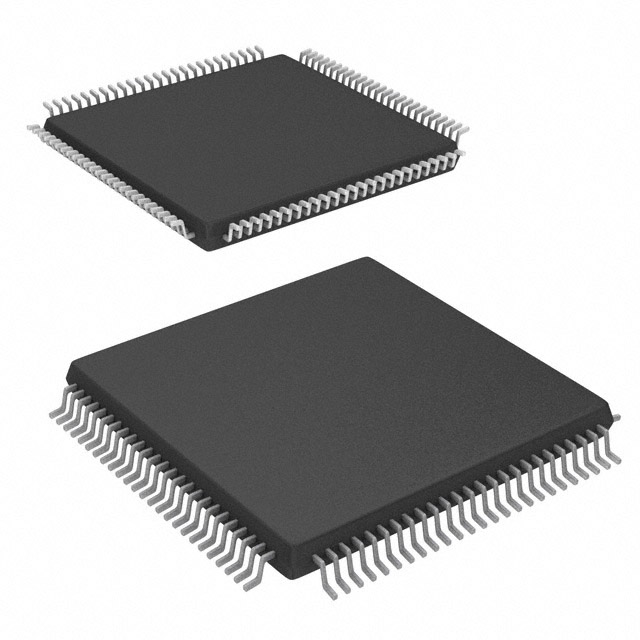
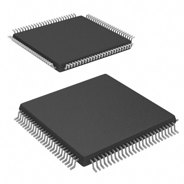
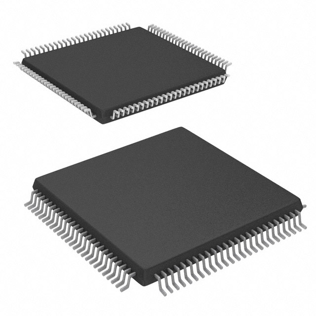
IGLOO nano Field Programmable Gate Array (FPGA) IC 68 36864 6144 100-TQFP |
|---|---|
| Quantity | 1,868 Available (as of October 7, 2026) |

| Product Category | Field Programmable Gate Array (FPGA) |
|---|---|
| Manufacturer | Microchip Technology |
| Manufacturing Status | Obsolete |
| Manufacturer Standard Lead Time | Contact Us |
| Datasheet |
Specifications & Environmental
| Device Package | 100-VQFP (14x14) | Grade | Commercial | Operating Temperature | -20°C – 85°C | ||
|---|---|---|---|---|---|---|---|
| Package / Case | 100-TQFP | Number of I/O | 68 | Voltage | 1.425 V - 1.575 V | ||
| Mounting Method | Surface Mount | RoHS Compliance | RoHS non-compliant | REACH Compliance | REACH Unaffected | ||
| Moisture Sensitivity Level | 3 (168 Hours) | Number of LABs/CLBs | 6144 | Number of Logic Elements/Cells | 6144 | ||
| Number of Gates | 250000 | ECCN | 3A991D | HTS Code | 8542.39.0001 | ||
| Qualification | N/A | Total RAM Bits | 36864 |
Overview of AGLN250V5-ZVQ100 – IGLOO nano FPGA, 250,000 gates, 68 I/Os, ~36 kbits RAM, 100‑TQFP
The AGLN250V5-ZVQ100 is an IGLOO nano low-power flash Field Programmable Gate Array (FPGA) from Microchip Technology. This surface-mount device provides 250,000 system gates realized as 6,144 logic elements, approximately 36 kbits of embedded RAM, and up to 68 user I/Os in a 100‑lead TQFP package.
Designed for power-conscious, reprogrammable system designs, the device supports flash-based nonvolatile configuration, mixed-voltage I/O operation and secure in-system programming—making it suitable for compact, low-power embedded systems and mixed-voltage interfacing tasks within commercial temperature ranges.
Key Features
- Logic Capacity — 6,144 logic elements (VersaTiles) delivering a 250,000-gate equivalent for implementing glue logic, control and moderate-complexity digital functions.
- Embedded Memory — Total on-chip RAM of 36,864 bits (approximately 36 kbits) provided in true dual-port SRAM block configurations for FIFOs and buffering.
- I/O Flexibility — 68 user I/Os with bank-selectable voltages and mixed-voltage support to interface with 1.2 V to 3.3 V domains as required by system peripherals.
- Low-Power Flash Technology — Flash-based configuration with Flash*Freeze capability for ultra-low power retention of FPGA content and instant-on support (series-level feature).
- Secure In-System Programming — Supports on-chip AES-based ISP and FlashLock mechanisms for secure configuration and protection of programmed content (series-level capability).
- Voltage and Temperature — Core supply range of 1.425 V to 1.575 V and an operating temperature range of −20 °C to +85 °C suitable for commercial-grade applications.
- Package & Mounting — 100‑lead TQFP (supplier package 100‑VQFP, 14×14 mm) in a surface-mount form factor for compact PCB layouts.
- Compliance — RoHS compliant, aligning with common environmental and manufacturability requirements.
Typical Applications
- Power-Sensitive Embedded Systems — Low-power flash architecture and Flash*Freeze capability enable use in devices where minimizing standby and active power is important.
- Mixed-Voltage Interfacing — Bank-selectable I/O voltages allow bridging and interfacing between different logic domains in compact system designs.
- Secure Reconfigurable Logic — On-chip AES ISP and FlashLock features support secure in-field updates and protected configuration storage for systems requiring controlled reprogramming.
- Compact Board-Level FPGA Integration — 100‑TQFP packaging and surface-mount mounting make the device suitable for space-constrained PCBs and single-chip solutions.
Unique Advantages
- High Logic Density in a Small Package: 250,000 gates and 6,144 logic elements provide substantial programmable logic capacity while maintaining a compact 100‑lead TQFP footprint.
- Nonvolatile, Secure Configuration: Flash-based storage retains design data without battery backup and supports secure in-system programming for update control and intellectual property protection.
- Flexible I/O and Mixed-Voltage Support: Up to 68 user I/Os with bank-selectable voltages simplify interfacing to a wide range of peripherals and sensors without extra level-shifting components.
- Engineered for Low Power: Flash*Freeze and low-voltage core operation reduce power consumption during active and retention modes, helping extend battery life in portable designs.
- Commercial Temperature Grade: Qualified for −20 °C to +85 °C operation to suit a broad set of commercial embedded applications.
- Manufacturability and Environmental Compliance: Surface-mount 100‑lead TQFP packaging and RoHS compliance support modern assembly processes and regulatory requirements.
Why Choose AGLN250V5-ZVQ100?
The AGLN250V5-ZVQ100 combines a flash-based, low-power FPGA architecture with moderate to high logic capacity and flexible I/O in a compact surface-mount TQFP package. It is positioned for designers needing reprogrammable, secure logic with low standby and active power characteristics, while retaining on-chip RAM for buffering and state storage.
This part is well suited to commercial embedded designs that require secure in-field updates, mixed-voltage interfacing, and a balance of logic density and compact board footprint. Its combination of flash configuration, embedded memory, and I/O flexibility provides a scalable, manufacturable solution for a range of reconfigurable logic tasks.
Request a quote or submit an inquiry to evaluate AGLN250V5-ZVQ100 for your next low-power, reprogrammable design.
























Date Founded: 1989
Headquarters: Chandler, Arizona, USA
Employees: 22,000+
Revenue: $8.349 Billion
Certifications and Memberships: ISO9001:2015, IATF16949:2016, AS 9100D




