
AT40K40AL-1BGC
| Part Description |
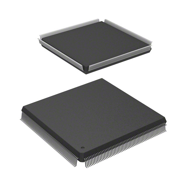
AT40KAL Field Programmable Gate Array (FPGA) IC 289 18432 2304 352-LBGA |
|---|---|
| Quantity | 42 Available (as of October 8, 2026) |

| Product Category | Field Programmable Gate Array (FPGA) |
|---|---|
| Manufacturer | Microchip Technology |
| Manufacturing Status | Obsolete |
| Manufacturer Standard Lead Time | Contact Us |
| Datasheet |
Specifications & Environmental
| Device Package | 352-SBGA (35x35) | Grade | Commercial | Operating Temperature | 0°C – 70°C | ||
|---|---|---|---|---|---|---|---|
| Package / Case | 352-LBGA | Number of I/O | 289 | Voltage | 3 V - 3.6 V | ||
| Mounting Method | Surface Mount | RoHS Compliance | RoHS non-compliant | REACH Compliance | REACH Unaffected | ||
| Moisture Sensitivity Level | 3 (168 Hours) | Number of LABs/CLBs | 2304 | Number of Logic Elements/Cells | 2304 | ||
| Number of Gates | 50000 | ECCN | 3A991D | HTS Code | 8542.39.0001 | ||
| Qualification | N/A | Total RAM Bits | 18432 |
Overview of AT40K40AL-1BGC – AT40KAL Field Programmable Gate Array (FPGA) IC, 289 I/Os, 18,432-bit RAM, 2,304 logic elements, 352-LBGA
The AT40K40AL-1BGC is an SRAM-based Field Programmable Gate Array (FPGA) designed for high-performance, reconfigurable logic applications. It implements the AT40KAL architecture with distributed on-chip SRAM, on-chip multipliers and support for dynamic partial or full reconfiguration (Cache Logic).
Targeted at systems requiring programmable DSP-style computation, coprocessing and high I/O density, this commercial-grade device offers a balance of logic capacity, embedded memory and flexible I/O in a 352-ball BGA package.
Key Features
- Core Performance – System speeds up to 100 MHz with array multipliers capable of >50 MHz and internal tri-state capability in each cell for flexible routing and logic implementation.
- Logic Capacity – 2,304 logic elements (cells) providing up to 50,000 gates of usable logic for mid‑to‑large sized designs.
- Embedded Memory (FreeRAM) – Distributed, flexible 10 ns SRAM totaling 18,432 bits usable for single/dual-port, synchronous or asynchronous memory functions without consuming logic resources.
- I/O and Clocking – 289 user I/Os with PCI-compliant capabilities, programmable output drive and up to 8 global clocks plus 4 dedicated PCI clocks for low-skew clock distribution and flexible timing control.
- Reconfiguration – Cache Logic dynamic partial/full reconfigurability and unlimited re-programmability via serial or parallel modes to support adaptive designs and in-system updates.
- Package and Supply – 352-LBGA / 352-SBGA (35×35) package; voltage supply 3.0 V to 3.6 V (3.3 V representative). Operating temperature range 0 °C to 70 °C. RoHS compliant.
- Design Integration – Industry tool flow compatibility and automatic component generators to accelerate synthesis, placement and routing for complex designs.
Typical Applications
- Signal Processing & DSP Coprocessors – Implement FIR filters, FFTs, convolvers and other arithmetic-heavy blocks to offload and accelerate processor workloads.
- Video and Multimedia Acceleration – Support for fast vector multipliers and distributed RAM enables compression/decompression and transform functions used in video pipelines.
- Security & Encryption – High logic density and embedded RAM allow hardware implementation of encryption cores and related cryptographic accelerators.
- High‑I/O System Interfaces – PCI-compliant I/Os and programmable drive strengths are suitable for designs requiring dense external interfacing and pin-locking flexibility.
Unique Advantages
- Dynamic In-System Reconfiguration – Cache Logic capability enables partial or full reconfiguration without loss of data, supporting adaptive and upgradable systems.
- On-Chip, Fast SRAM – Approximately 18,432 bits of distributed 10 ns RAM reduce dependence on external memory and preserve logic resources for higher‑level functions.
- Balanced Performance and Capacity – Combines 2,304 logic elements with up to 50,000 gates and high-speed multipliers for compute-intensive applications.
- Robust Clocking Resources – Eight global clocks and additional PCI clocks deliver low-skew distribution and flexible edge/transition control for complex timing domains.
- Compact, High-Density Packaging – 352-ball BGA package provides high pin count and board-level density for designs constrained by PCB real estate.
Why Choose AT40K40AL-1BGC?
The AT40K40AL-1BGC positions itself as a versatile, mid-to-high capacity FPGA optimized for designs that need a combination of embedded RAM, fast multipliers and in-system reconfigurability. Its feature set is oriented toward engineers developing DSP acceleration, multimedia processing and high‑I/O interface logic where reprogrammability and on-chip memory reduce system complexity.
With commercial operating range, RoHS compliance, and a 352-ball BGA footprint, this device addresses projects that require dense I/O, deterministic performance and flexible update mechanisms while supporting standard 3.3 V system environments.
Request a quote or submit an inquiry to receive pricing and availability for the AT40K40AL-1BGC. Our team can provide lead-time details and support for volume requirements.























Date Founded: 1989
Headquarters: Chandler, Arizona, USA
Employees: 22,000+
Revenue: $8.349 Billion
Certifications and Memberships: ISO9001:2015, IATF16949:2016, AS 9100D




