
AT40K40-2FQC
| Part Description |
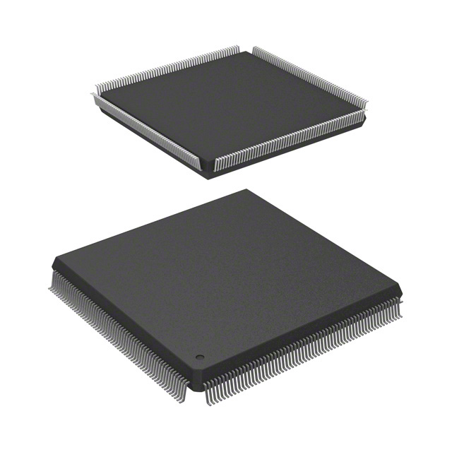
AT40K/KLV Field Programmable Gate Array (FPGA) IC 256 18432 2304 304-BFQFP |
|---|---|
| Quantity | 168 Available (as of June 10, 2026) |

| Product Category | Field Programmable Gate Array (FPGA) |
|---|---|
| Manufacturer | Microchip Technology |
| Manufacturing Status | Obsolete |
| Manufacturer Standard Lead Time | Contact Us |
| Datasheet |
Specifications & Environmental
| Device Package | 304-PQFP (40x40) | Grade | Commercial | Operating Temperature | 0°C – 70°C | ||
|---|---|---|---|---|---|---|---|
| Package / Case | 304-BFQFP | Number of I/O | 256 | Voltage | 4.75 V - 5.25 V | ||
| Mounting Method | Surface Mount | RoHS Compliance | RoHS non-compliant | REACH Compliance | REACH Unaffected | ||
| Moisture Sensitivity Level | 3 (168 Hours) | Number of LABs/CLBs | 2304 | Number of Logic Elements/Cells | 2304 | ||
| Number of Gates | 50000 | ECCN | 3A991D | HTS Code | 8542.39.0001 | ||
| Qualification | N/A | Total RAM Bits | 18432 |
Overview of AT40K40-2FQC – Field Programmable Gate Array (FPGA), 2,304 logic elements, 18,432-bit RAM, 256 I/O, 304-BFQFP
The AT40K40-2FQC is an SRAM-based FPGA from Microchip Technology designed for high-performance, reconfigurable digital logic. As part of the AT40K series, this device combines 2,304 logic elements with distributed on-chip RAM and a rich I/O complement for mid-range gate-count FPGA applications.
Targeted at systems that require performance and in-system adaptability, the AT40K40-2FQC offers system speeds up to 100 MHz, PCI-compliant I/O capability, and features that support DSP-style coprocessing, multimedia processing, and adaptive logic updates. It operates from a 4.75 V to 5.25 V supply and is specified for commercial temperature operation (0 °C to 70 °C).
Key Features
- Core Performance – Up to 2,304 logic elements (cells) enabling designs in the ~40K–50K usable-gate range; system speeds to 100 MHz and array multipliers >50 MHz as specified for the series.
- Distributed On-Chip RAM (FreeRAM) – Up to 18,432 bits of flexible, 10 ns programmable SRAM that can be instantiated as single- or dual-port, synchronous or asynchronous memory without consuming logic resources.
- I/O and Interface Capability – 256 I/O pins with PCI-compliant I/O support and 3 V/5 V signaling capability in the series; programmable output drive and fast, flexible array access to aid pin locking and board-level integration.
- Clocking and Timing – Eight global clocks with low-skew distribution and programmable edge transitions, plus four additional dedicated PCI clocks for synchronous system designs.
- Reconfigurability – Series-level Cache Logic capability enables dynamic full or partial in-system reconfiguration with unlimited reprogramming via serial or parallel modes for adaptive designs.
- Package and Mounting – Surface-mount 304-BFQFP package (supplier device package: 304-PQFP, 40 × 40 mm) suitable for compact board-level integration.
- Supply and Temperature – 5 V supply range (4.75 V to 5.25 V) and commercial-grade operating temperature from 0 °C to 70 °C.
- Compliance – RoHS-compliant device; series documented as fully PCI-compliant in the datasheet content.
Typical Applications
- DSP Coprocessor – Implement FIR filters, FFTs and other arithmetic accelerators using the device’s array multipliers and distributed RAM for high-throughput signal processing.
- Video and Multimedia Processing – Use on-chip multipliers and fast SRAM to accelerate video compression/decompression, DCT operations, and real-time media algorithms.
- PCI-Based Systems – Integrate as a programmable logic element in PCI-compliant designs where flexible I/O and dedicated PCI clocks simplify board-level interfacing.
- Adaptive and Reconfigurable Systems – Leverage Cache Logic dynamic reconfigurability for systems that require in-field updates or rapid algorithm changes without full device replacement.
Unique Advantages
- Balanced Performance and Capacity: 2,304 logic elements and approximately 18,432 bits of distributed SRAM provide a mid-range gate-count solution for complex logic and embedded memory needs.
- Fast, Deterministic Memory: 10 ns FreeRAM blocks enable low-latency embedded memory implementations for FIFOs, scratch pads, and coefficient storage without consuming logic elements.
- Robust Clocking: Eight global clocks and programmable edge transitions reduce clock distribution challenges and enable low-skew synchronous designs.
- Field Reconfigurability: Series-level support for unlimited serial/parallel reprogramming and partial in-system reconfiguration allows rapid updates and adaptive system behavior.
- Practical Board Integration: 256 I/Os, programmable output drive, and a 304-pin PQFP/BFQFP package simplify routing and signal integrity planning for dense designs.
- Commercial-Grade Reliability: Specified for 0 °C to 70 °C operation and RoHS compliance for mainstream commercial applications.
Why Choose AT40K40-2FQC?
The AT40K40-2FQC delivers a practical mix of logic density, embedded memory, and system-level features—including high-speed operation, multiple global clocks, and in-system reconfiguration—making it well suited for mid-range FPGA applications that demand both performance and flexibility. Its PCI-compliant I/O characteristics and abundant on-chip RAM support DSP acceleration and media processing tasks while simplifying board integration.
This device is a good fit for design teams and system integrators building commercial electronic products that require reprogrammable hardware, embedded memory resources, and deterministic timing behavior, with supply voltage and thermal specifications aligned to standard commercial environments.
Request a quote or submit an RFQ to obtain pricing, availability and lead-time details for the AT40K40-2FQC.


Date Founded: 1989
Headquarters: Chandler, Arizona, USA
Employees: 22,000+
Revenue: $8.349 Billion
Certifications and Memberships: ISO9001:2015, IATF16949:2016, AS 9100D


