
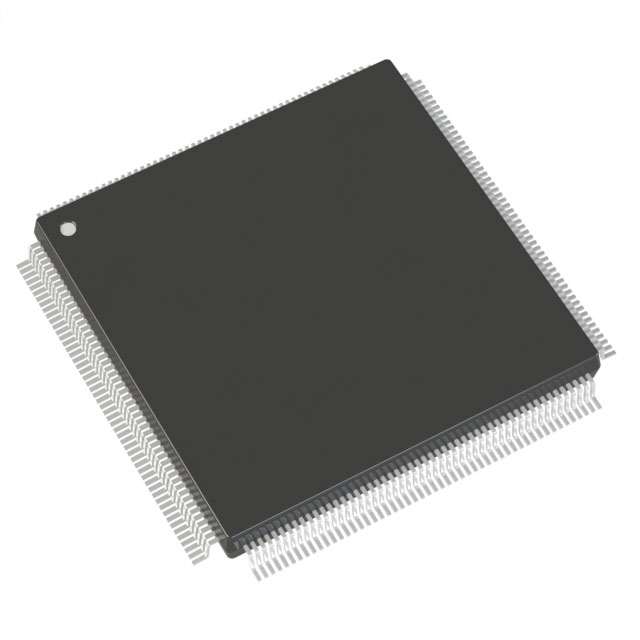
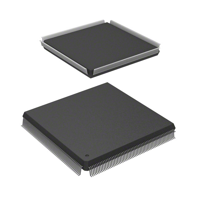
AT40K40-2DQC
| Part Description |
AT40K/KLV Field Programmable Gate Array (FPGA) IC 161 18432 2304 208-BFQFP |
|---|---|
| Quantity | 68 Available (as of June 15, 2026) |

| Product Category | Field Programmable Gate Array (FPGA) |
|---|---|
| Manufacturer | Microchip Technology |
| Manufacturing Status | Active |
| Manufacturer Standard Lead Time | 52 Weeks |
| Datasheet |
Specifications & Environmental
| Device Package | 208-PQFP (28x28) | Grade | Commercial | Operating Temperature | 0°C – 70°C | ||
|---|---|---|---|---|---|---|---|
| Package / Case | 208-BFQFP | Number of I/O | 161 | Voltage | 4.75 V - 5.25 V | ||
| Mounting Method | Surface Mount | RoHS Compliance | RoHS non-compliant | REACH Compliance | REACH Unaffected | ||
| Moisture Sensitivity Level | 3 (168 Hours) | Number of LABs/CLBs | 2304 | Number of Logic Elements/Cells | 2304 | ||
| Number of Gates | 50000 | ECCN | 3A991D | HTS Code | 8542.39.0001 | ||
| Qualification | N/A | Total RAM Bits | 18432 |
Overview of AT40K40-2DQC – AT40K/KLV Field Programmable Gate Array (FPGA) IC 161 18432 2304 208-BFQFP
The AT40K40-2DQC is an SRAM-based Field Programmable Gate Array (FPGA) in the AT40K family, designed for high-performance, reconfigurable logic applications. As a member of the AT40K/AT40KLV family, it combines distributed on-chip SRAM, global clock resources and reconfiguration capabilities to support compute-intensive and interface-driven designs.
This device targets commercial embedded systems, communication and multimedia designs that require flexible memory, abundant I/O and substantial gate density—delivered in a 208-pin PQFP surface-mount package and powered from a 4.75 V to 5.25 V supply.
Key Features
- Core Capacity — 2,304 logic elements (cells) supporting approximately 50,000 gates of usable logic to implement mid-range FPGA designs.
- Distributed On-Chip Memory (FreeRAM™) — 18,432 bits of flexible, 10 ns SRAM distributed across the fabric for single- or dual-port, synchronous/asynchronous memory functions.
- I/O and Interface — 161 I/O pins in a pin-compatible package range; family-level PCI-compliant I/O options and programmable output drive enable flexible interfacing.
- Clocking — Eight global clocks with low-skew distribution and programmable edge transitions to support synchronous designs and clock management strategies.
- Reconfigurability — Cache Logic dynamic full/partial in-system reconfigurability (family feature) enabling unlimited re-programmability via serial or parallel modes for adaptive designs.
- Performance — Family-level system speeds up to 100 MHz, array multipliers >50 MHz and 10 ns SRAM timing for high-throughput arithmetic and data-path implementations.
- Package & Mounting — 208-PQFP (28×28 mm) plastic quad flat pack, surface-mount mounting for standard PCB assembly processes.
- Supply & Temperature — 4.75 V to 5.25 V operating supply; commercial operating temperature range 0 °C to 70 °C.
- Toolchain Integration — Family-level support for industry-standard design tools and flows to streamline synthesis, placement, routing and IP integration.
- RoHS Compliant — Device meets RoHS environmental requirements.
Typical Applications
- DSP and Coprocessing — Implement arithmetic-intensive functions (FIR filters, FFTs, multipliers) using the device’s fast array multipliers and distributed SRAM as a coprocessor alongside a host CPU.
- Video and Multimedia Processing — Use on-chip memory and reconfigurable logic for tasks such as video compression/decompression and fast vector multiplier updates.
- Embedded I/O and Interface Bridging — Leverage 161 I/Os and programmable drive strength for protocol adaptation, bus interfacing and custom peripheral glue logic.
- Adaptive and Updatable Systems — Take advantage of in-system reconfigurability to update algorithms or coefficients without removing the device from the board.
Unique Advantages
- Balanced Logic and Memory — 2,304 logic elements paired with 18,432 bits of distributed SRAM delivers a compact mix of logic and embedded memory for mid-range systems.
- Flexible Memory Architecture — Distributed 10 ns SRAM can be instantiated as single- or dual-port, synchronous or asynchronous memory blocks for FIFOs, scratch pads and buffers without consuming separate logic resources.
- Robust Clocking Resources — Eight global clocks and programmable edge control simplify timing-sensitive designs and reduce clock distribution complexity.
- Reconfigurable Design Lifecycle — Dynamic full/partial reconfiguration supports adaptive designs and rapid in-system updates to accelerate development and field upgrades.
- Commercial-Grade Integration — 208-PQFP packaging, surface-mount mounting and a standard 5 V supply make the device straightforward to integrate into commercial embedded boards.
- Proven Design Flow Compatibility — Industry-standard tool support aids in fast synthesis, placement/routing and IP integration to shorten design cycles.
Why Choose AT40K40-2DQC?
The AT40K40-2DQC delivers a practical combination of mid-range gate count, distributed on-chip memory and flexible I/O in a commercial 208-pin PQFP package. Its architecture—featuring fast SRAM, multiple global clocks and in-system reconfigurability—makes it well suited for DSP acceleration, interface bridging and adaptive embedded applications where field updates and memory-efficient implementations matter.
This FPGA is ideal for design teams that need predictable 5 V supply operation, a clear migration path within the AT40K family, and compatibility with established synthesis and verification toolchains to accelerate time-to-market while maintaining design flexibility.
Request a quote or submit an inquiry to receive pricing, lead-time and availability information for the AT40K40-2DQC. Our team will respond with the details you need to move your design forward.


Date Founded: 1989
Headquarters: Chandler, Arizona, USA
Employees: 22,000+
Revenue: $8.349 Billion
Certifications and Memberships: ISO9001:2015, IATF16949:2016, AS 9100D


