
AT40K20LV-3DQI
| Part Description |
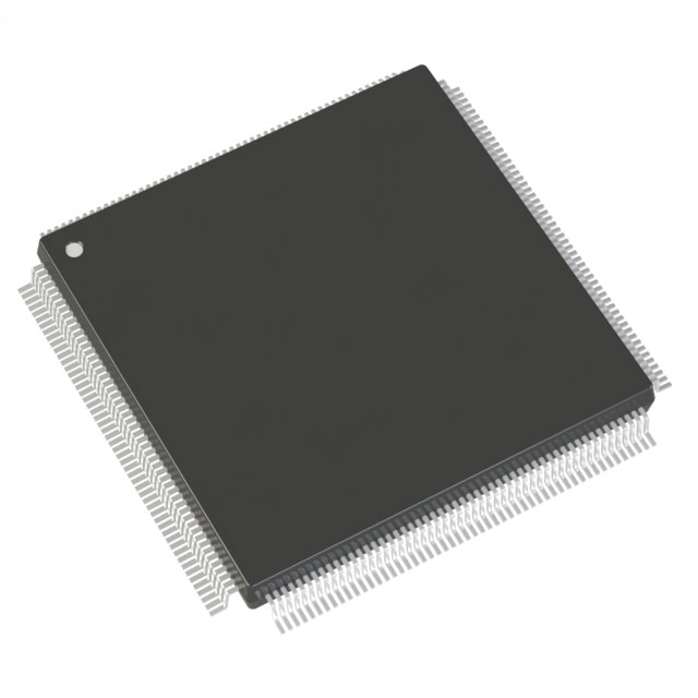
AT40K/KLV Field Programmable Gate Array (FPGA) IC 161 8192 1024 208-BFQFP |
|---|---|
| Quantity | 734 Available (as of June 18, 2026) |
| Product Category | Field Programmable Gate Array (FPGA) |
|---|---|
| Manufacturer | Microchip Technology |
| Manufacturing Status | Obsolete |
| Manufacturer Standard Lead Time | Contact Us |
| Datasheet |
Specifications & Environmental
| Device Package | 208-PQFP (28x28) | Grade | Industrial | Operating Temperature | -40°C – 85°C | ||
|---|---|---|---|---|---|---|---|
| Package / Case | 208-BFQFP | Number of I/O | 161 | Voltage | 3 V - 3.6 V | ||
| Mounting Method | Surface Mount | RoHS Compliance | RoHS non-compliant | REACH Compliance | REACH Unaffected | ||
| Moisture Sensitivity Level | 3 (168 Hours) | Number of LABs/CLBs | 1024 | Number of Logic Elements/Cells | 1024 | ||
| Number of Gates | 30000 | ECCN | 3A991D | HTS Code | 8542.39.0001 | ||
| Qualification | N/A | Total RAM Bits | 8192 |
Overview of AT40K20LV-3DQI – 3 V–3.6 V, 1,024 Logic-Element FPGA, 208-BFQFP
The AT40K20LV-3DQI is an SRAM-based field programmable gate array (FPGA) in the AT40K/AT40KLV family, offering 1,024 logic elements and 8,192 bits of on-chip RAM in a 208-BFQFP package. Designed for industrial applications, this device provides a mid-range gate count solution with 161 I/O pins and a 3 V–3.6 V supply range.
As part of the AT40KLV series, the device benefits from the family’s distributed 10 ns programmable SRAM, multiple global clocks and dynamic reconfiguration capabilities, making it suitable for computation-intensive and reconfigurable embedded designs.
Key Features
- Logic Capacity — 1,024 logic elements (cells) and approximately 30,000 usable gates for mid-range FPGA designs.
- Embedded Memory (FreeRAM) — 8,192 bits of distributed SRAM supporting flexible single/dual-port and synchronous/asynchronous configurations with 10 ns access characteristics.
- I/O and Drive — 161 I/O pins providing extensive external interfacing; family-level support for programmable output drive and 3 V/5 V capability.
- Clocking — Family features include up to 8 global clocks and additional dedicated PCI clocks for low-skew distribution and flexible clock management.
- Performance Characteristics — Series-level capabilities include system speeds to 100 MHz and array multiplier performance exceeding 50 MHz; 10 ns flexible SRAM and internal tri-state capability in each cell.
- Package & Mounting — Supplied in a 208-BFQFP (208-PQFP, 28×28) surface-mount package suitable for standard PCB assembly flows.
- Power & Temperature — Voltage supply range 3 V to 3.6 V, operating temperature −40 °C to 85 °C, rated for industrial-grade environments.
- Compliance — RoHS compliant for lead-free manufacturing requirements.
Typical Applications
- DSP Coprocessors — Implement arithmetic-intensive functions such as FIR filters and FFTs to offload processing from host CPUs in embedded systems.
- Multimedia & Video Processing — Support for array multipliers and distributed RAM makes the device suitable for video compression/decompression and related multimedia pipelines.
- Encryption & Security Engines — Reconfigurable logic and embedded RAM enable implementation of encryption, hashing and other security accelerators.
- Adaptive Signal Processing — Cache Logic and in-system reconfigurability facilitate adaptive filter updates and algorithm tuning without removing the device from the system.
Unique Advantages
- Balanced Mid-Range Capacity: 1,024 logic elements with ~30,000 gates provide a practical balance between resource availability and cost for mid-complexity designs.
- Flexible On-Chip Memory: 8,192 bits of distributed FreeRAM enable multiple independent single/dual-port RAM structures without consuming logic resources.
- Robust I/O Count: 161 I/Os allow extensive external connectivity for interfaces, peripherals and multi-board systems.
- Industrial Temperature Range: Rated for −40 °C to 85 °C for reliable operation in industrial environments.
- Reconfiguration Capabilities: Family-level Cache Logic and in-system reprogrammability support adaptive designs and rapid updates in the field.
- Industry Toolchain Integration: The AT40K/AT40KLV series integrates with established synthesis and simulation flows to accelerate development and verification.
Why Choose AT40K20LV-3DQI?
The AT40K20LV-3DQI delivers a practical and versatile FPGA option for systems that require mid-range logic capacity, distributed on-chip RAM and a substantial I/O complement in a 208-BFQFP package. Its 3 V–3.6 V supply compatibility and industrial temperature rating position it well for embedded, industrial and reconfigurable processing applications.
Engineers targeting DSP acceleration, adaptive signal processing, multimedia processing or security acceleration will find the AT40K20LV-3DQI offers a combination of memory flexibility, clocking options and reconfiguration features that support iterative design and in-system updates while maintaining a manageable BOM and form factor.
Request a quote or submit your request for quotation to our team for pricing and availability of the AT40K20LV-3DQI. Our sales group can provide lead times and order support tailored to your project needs.


Date Founded: 1989
Headquarters: Chandler, Arizona, USA
Employees: 22,000+
Revenue: $8.349 Billion
Certifications and Memberships: ISO9001:2015, IATF16949:2016, AS 9100D


