
AT40K40-2BGI
| Part Description |
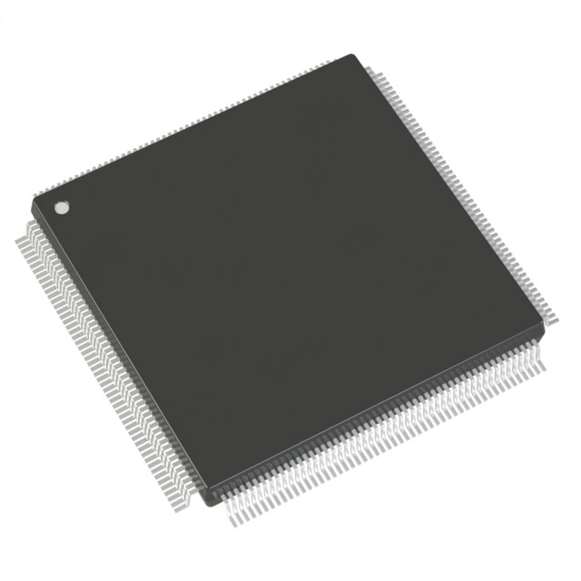
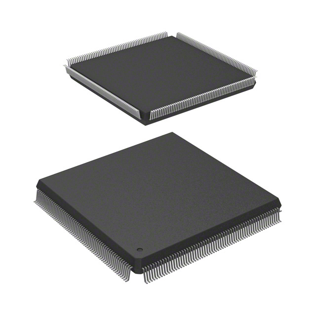
AT40K/KLV Field Programmable Gate Array (FPGA) IC 289 18432 2304 352-LBGA |
|---|---|
| Quantity | 715 Available (as of October 7, 2026) |

| Product Category | Field Programmable Gate Array (FPGA) |
|---|---|
| Manufacturer | Microchip Technology |
| Manufacturing Status | Obsolete |
| Manufacturer Standard Lead Time | Contact Us |
| Datasheet |
Specifications & Environmental
| Device Package | 352-SBGA (35x35) | Grade | Industrial | Operating Temperature | -40°C – 85°C | ||
|---|---|---|---|---|---|---|---|
| Package / Case | 352-LBGA | Number of I/O | 289 | Voltage | 4.5 V - 5.5 V | ||
| Mounting Method | Surface Mount | RoHS Compliance | RoHS non-compliant | REACH Compliance | REACH Unaffected | ||
| Moisture Sensitivity Level | 3 (168 Hours) | Number of LABs/CLBs | 2304 | Number of Logic Elements/Cells | 2304 | ||
| Number of Gates | 50000 | ECCN | 3A991D | HTS Code | 8542.39.0001 | ||
| Qualification | N/A | Total RAM Bits | 18432 |
Overview of AT40K40-2BGI – AT40K/KLV Field Programmable Gate Array, 352-LBGA, 4.5–5.5 V
The AT40K40-2BGI is an SRAM-based Field Programmable Gate Array (FPGA) in a 352-ball LBGA package designed for high-performance, reconfigurable logic. It provides 2,304 logic elements, approximately 50,000 usable gates and 18,432 bits of distributed on-chip RAM, targeting mid-to-high gate-count designs that require embedded memory and fast arithmetic resources.
Built with features such as FreeRAM distributed SRAM, eight global clocks and dynamic Cache Logic reconfigurability, the device is suitable for DSP co-processing, multimedia processing and PCI-compliant system designs operating over a 4.5 V to 5.5 V supply and an industrial temperature range of −40 °C to 85 °C.
Key Features
- Core Logic 2,304 logic elements (cells) providing approximately 50,000 gates of usable logic capacity for medium to large designs.
- Embedded Memory (FreeRAM) Distributed, flexible single/dual-port SRAM totaling 18,432 bits; 10 ns SRAM timing supports synchronous or asynchronous operation for FIFOs and scratch-pad memory.
- I/O and Interface Up to 289 I/Os with 3V/5V capability, programmable output drive and fast array access to facilitate pin locking and PCI-compliant implementations.
- Clocking Eight global clocks with low-skew distribution, programmable edge transitions, distributed clock shutdown and additional dedicated PCI clocks for synchronous system architectures.
- Reconfiguration & Cache Logic Dynamic full/partial reconfigurability in-system with unlimited re-programmability via serial or parallel modes, enabling adaptive designs and fast coefficient updates.
- Arithmetic Performance Cell-to-cell connections and architecture optimized for fast array and vector multipliers and system speeds cited up to 100 MHz for common implementations.
- Package & Mounting Surface-mount 352-LBGA package (352-SBGA, 35×35) for high-density board integration.
- Power & Temperature Operational supply range 4.5 V to 5.5 V with an industrial operating temperature range of −40 °C to 85 °C.
- Design Tool Integration Works with industry-standard synthesis, simulation and place-and-route tools cited in the datasheet for streamlined development and back-annotation workflows.
- Standards Compliance PCI-compliant I/O support to facilitate integration into PCI-based systems.
- RoHS Compliant Manufactured in compliance with RoHS requirements.
Typical Applications
- DSP Acceleration Use as a coprocessor for computation-intensive functions such as FIR filters, FFTs and vector multipliers to offload processors and accelerate signal processing pipelines.
- Video and Multimedia Processing Implement convolution, compression/decompression and discrete-cosine transform (DCT) engines using the device’s embedded multipliers and distributed memory.
- Secure Systems Hardware-accelerated encryption and data processing blocks leveraging the FPGA’s reconfigurability and embedded RAM for key storage and buffer operations.
- PCI-Backed System Integration Deploy in PCI-compliant designs that require flexible I/O drive levels and dedicated PCI clocks for reliable interfacing.
Unique Advantages
- High Logic Density: 2,304 logic elements and ~50,000 gates deliver the capacity needed for complex logic and DSP-heavy designs without external gate arrays.
- Flexible On-Chip Memory: Distributed FreeRAM (up to 18,432 bits) supports multiple independent single- or dual-port RAM blocks for FIFOs, buffers and parameter storage.
- In-System Reconfigurability: Cache Logic enables full or partial dynamic reconfiguration in-system with unlimited re-programmability for adaptive and updateable designs.
- Robust Clocking: Eight global clocks with low skew and programmable edges simplify synchronous design and power management through distributed clock shutdown.
- Industry Toolchain Support: Compatibility with industry-standard design and synthesis tools accelerates development and aids migration from existing FPGA flows.
- Industrial Temperature Range: Rated for −40 °C to 85 °C operation to meet temperature requirements for many embedded and industrial applications.
Why Choose AT40K40-2BGI?
The AT40K40-2BGI positions itself as a versatile, mid-to-high gate-count FPGA that combines substantial embedded memory, flexible I/O and dynamic reconfiguration features suitable for DSP acceleration, multimedia processing and PCI-based systems. Its 352-LBGA package and surface-mount mounting make it appropriate for compact, board-level integration where logic density and embedded RAM are required.
Supported by a set of industry-standard design tools and featuring PCI-compliant I/Os and robust clocking resources, this device is suited for designers who need adaptable hardware to implement arithmetic-intensive functions, update systems in-field and integrate with proven development workflows.
Request a quote or submit a quote to evaluate AT40K40-2BGI for your next FPGA-based design.
























Date Founded: 1989
Headquarters: Chandler, Arizona, USA
Employees: 22,000+
Revenue: $8.349 Billion
Certifications and Memberships: ISO9001:2015, IATF16949:2016, AS 9100D




