
AT40K40-2DQI
| Part Description |
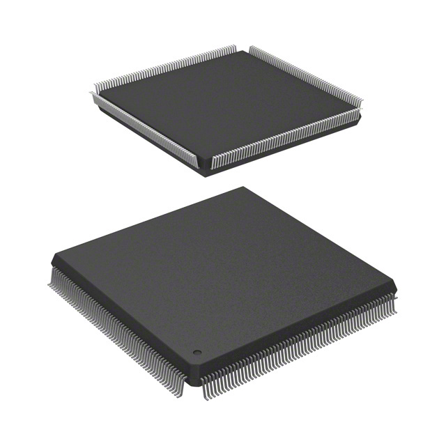
AT40K/KLV Field Programmable Gate Array (FPGA) IC 161 18432 2304 208-BFQFP |
|---|---|
| Quantity | 162 Available (as of October 8, 2026) |

| Product Category | Field Programmable Gate Array (FPGA) |
|---|---|
| Manufacturer | Microchip Technology |
| Manufacturing Status | Obsolete |
| Manufacturer Standard Lead Time | Contact Us |
| Datasheet |
Specifications & Environmental
| Device Package | 208-PQFP (28x28) | Grade | Industrial | Operating Temperature | -40°C – 85°C | ||
|---|---|---|---|---|---|---|---|
| Package / Case | 208-BFQFP | Number of I/O | 161 | Voltage | 4.5 V - 5.5 V | ||
| Mounting Method | Surface Mount | RoHS Compliance | RoHS non-compliant | REACH Compliance | REACH Unaffected | ||
| Moisture Sensitivity Level | 3 (168 Hours) | Number of LABs/CLBs | 2304 | Number of Logic Elements/Cells | 2304 | ||
| Number of Gates | 50000 | ECCN | 3A991D | HTS Code | 8542.39.0001 | ||
| Qualification | N/A | Total RAM Bits | 18432 |
Overview of AT40K40-2DQI – AT40K/KLV Field Programmable Gate Array (FPGA), 2,304 logic elements, 18,432-bit SRAM, 161 I/Os, 208-BFQFP
The AT40K40-2DQI is an SRAM-based FPGA from the AT40K family, offering 2,304 logic elements, approximately 18,432 bits of distributed on-chip RAM, and 161 I/O pins in a 208-BFQFP package. It operates from a 4.5 V to 5.5 V supply and is specified for industrial temperature operation from -40 °C to 85 °C.
Designed for high-performance embedded and DSP-augmented systems, the device provides features such as fast on-chip SRAM, dedicated clock resources and in-system reconfigurability. Typical applications include coprocessor acceleration, multimedia processing, and other compute-intensive tasks where reprogrammable logic and embedded RAM accelerate algorithm execution.
Key Features
- Core Capacity 2,304 logic elements and a stated gate-equivalent figure of 50,000 gates provide capacity for medium-complexity FPGA designs.
- Embedded Memory (FreeRAM) Approximately 18,432 bits of distributed, 10 ns SRAM usable in single- or dual-port configurations; memory is independent of logic resources to maximize flexibility.
- High-Speed Building Blocks Series-level performance notes include system speeds to 100 MHz and array multipliers > 50 MHz, plus a 10 ns programmable SRAM access time for responsive data handling.
- I/O and Interface 161 I/O pins with 3V/5V capability and programmable output drive; the series supports PCI-compliant I/Os per datasheet guidance.
- Clocking Eight global clocks with low-skew distribution, programmable edge transitions and distributed clock shutdown for power management.
- Reconfigurability Cache Logic support for dynamic full or partial in-system reconfiguration with unlimited re-programmability via serial or parallel modes.
- Package & Mounting 208-BFQFP (supplier package 208-PQFP, 28 × 28) in a surface-mount format suitable for standard PCB assembly.
- Power & Environmental 5 V-class device operation with supply range 4.5 V to 5.5 V and industrial-grade operating temperature from -40 °C to 85 °C.
- Compliance RoHS compliant.
Typical Applications
- Coprocessor Acceleration Offload compute-heavy functions (FIR filters, FFTs, multipliers) to on-chip logic and RAM for higher system throughput.
- Multimedia Processing Use the device’s array multipliers and distributed SRAM to implement video compression, decompression and other signal-processing kernels.
- High-Speed Embedded Systems Deploy as a reconfigurable accelerator in DSP/processor-based platforms to implement arithmetic and control functions with low-latency on-chip memory access.
- PCI-Related Interfaces Leverage the series’ PCI-compliant I/O capability and programmable output drive when integrating with PCI-based systems or legacy 3.3 V/5 V interfaces.
Unique Advantages
- Integrated On-Chip SRAM: Approximately 18,432 bits of distributed FreeRAM that can be instantiated as single- or dual-port memory without consuming additional logic resources.
- Fast, Deterministic Performance: Series-level system speeds to 100 MHz and 10 ns SRAM access provide deterministic timing for demanding signal-processing tasks.
- Flexible In-System Reconfiguration: Cache Logic enables full or partial reconfiguration in-system via serial or parallel modes for adaptive designs and field updates.
- Industrial Operating Range: Specified operation from -40 °C to 85 °C and RoHS compliance support deployment in industrial applications.
- Standard Surface-Mount Package: 208‑pin BFQFP (28 × 28 PQFP footprint) eases PCB design and assembly for space- and cost-constrained systems.
- 3V/5V I/O Flexibility: I/O capability supports mixed-voltage interfacing and programmable output drive to simplify integration with existing boards and subsystems.
Why Choose AT40K40-2DQI?
The AT40K40-2DQI positions itself as a mid-density, industrial-temperature FPGA that combines 2,304 logic elements with sizable distributed SRAM and flexible I/O for applications needing reprogrammable acceleration and on-chip memory. Its combination of fast SRAM, dedicated clocking resources and in-system reconfiguration makes it well suited for embedded DSP, multimedia and coprocessing roles.
For teams seeking predictable performance in 5 V-class environments and a standard 208-pin PQFP footprint, the AT40K40-2DQI offers a practical balance of capacity, on-chip memory and system-level features aligned to established toolchains and design flows referenced in the AT40K series documentation.
If you need pricing, lead-time information or a formal quote for the AT40K40-2DQI, request a quote or submit an inquiry to receive details on availability and ordering.























Date Founded: 1989
Headquarters: Chandler, Arizona, USA
Employees: 22,000+
Revenue: $8.349 Billion
Certifications and Memberships: ISO9001:2015, IATF16949:2016, AS 9100D




